Mastering the bend: Essential tips & tricks for rigid-flex PCB design

PCB design starts in a mechanical world! This mechanical “domain” dictates the envelope in which a PCB design is to be created and function within this allotted physical constraint. Ever found yourself wrestling with space constraints or reliability issues in a compact device? That’s where Rigid-Flex PCBs step in like a superhero, offering the best of both worlds: the robust component support of rigid boards and the dynamic flexibility of flexible circuits. They’re a game-changer for everything from medical devices, to automotive, and aerospace applications!
But, as with any advanced technology, getting rigid-flex PCB design right requires a little know-how. To help you navigate the exciting world of bendable electronics, I’ve put together some essential tips and tricks. Let’s dive in!

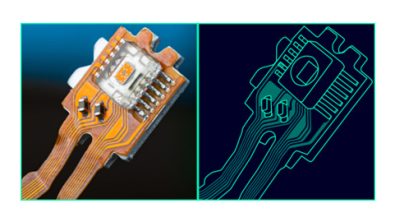
(Image courtesy of Iconnect007 and ASC)
Understanding rigid-flex: A quick refresher
Before we get to the tips, let’s quickly recap. Rigid-flex PCBs integrate rigid circuit board sections with flexible circuit sections, connected through plated through-holes. This allows for dynamic flexing during operation or static flexing for installation, eliminating connectors, reducing weight, and boosting reliability. Pretty neat, right?
Design phase: Laying the foundation for success
The magic of rigid-flex truly begins in the design phase. A little extra thought here can save you a lot of headaches (and costs!) down the line. Industry’s best practice is to establish and maintain close collaboration with your PCB fabricator. It’s even more so when implementing Rigid-Flex technology into your design. It’s paramount!
Mind the bend radius – It’s crucial!
- The golden rule: This is perhaps the most critical aspect. Every flexible material has a minimum bend radius it can safely tolerate without damage. Pushing it too far can lead to cracked traces or delamination.
- Dynamic vs. static: For designs that will flex repeatedly (dynamic), you’ll need a much larger bend radius than for those that flex only once for installation (static).
- Recommendation: Always consult your material supplier’s datasheet as well as your fabricator for specific bend radius recommendations. A general rule of thumb for dynamic flexing is at least 10x the flex material’s thickness.
Layer stack-up: The art of transition
- Symmetry is key: Aim for a symmetrical stack-up in the flexible sections to prevent warping and stress during bending.
- Gradual transitions: Where the rigid and flex sections meet, ensure a smooth transition. Avoid abrupt changes in thickness or material.
- Copper weight: Use thinner copper (e.g., 0.5 oz or 1 oz) for flex layers, especially in bending areas, as it’s more flexible.
Trace routing in flex areas: Attention to detail is key here!
- Avoid sharp angles: Never route traces at 90-degree angles in flex areas. Use gentle curves or teardrops to minimize stress concentration. Think of it like a river: it flows smoothly, not in sharp turns!
- Perpendicular traces: Route traces perpendicular to the bend line whenever possible. This distributes stress more evenly across the trace width.
- Staggered traces: If you have multiple traces, stagger them rather than stacking them directly on top of each other to avoid the I-beam effect. This prevents localized stress points.
- Cross-hatching ground/power planes: In flex areas, use cross-hatched or solid copper with relief cuts for ground and power planes instead of solid copper. This improves flexibility. If impedance is required, use a mixed solid and hatch plane approach, where a small portion of a sold reference (GND) shape, about 2x the signal trace width, is applied only along the adjacent reference layer immediately under the signal trace, so that the signal trace maintains its reference to the reference plane. This technique eliminates any potential impedance discontinuities over the flex section that may stem from routing a signal trace over a hatch reference plan in the design.
Component placement: Keep it clear!
- No Components in bend areas: This might seem obvious, but it’s worth reiterating. Components, vias, and even through-holes should be kept well away from any area that will flex.
- Component-to-flex transition: Maintain sufficient clearance between the last component on the rigid board and the start of the flex section.
Material selection: The right fit (fabricator collaboration is key!)
- Polyimide (PI): This is the most common and robust material for flex circuits, offering excellent thermal and mechanical properties.
- Adhesives: Choose adhesives carefully, as they significantly impact flexibility and reliability. Acrylic-based adhesives are common.
- Stiffeners/coverlays: Use stiffeners (like FR-4 or polyimide) on flex sections where components are mounted or for connector support. Coverlays (like polyimide or liquid photoimageable solder mask) protect the traces on the flex layers.
Manufacturing phase: Bringing your design to life
Even the best design needs careful manufacturing. Here are a few points to consider:
- Panelization for Efficiency: If you are designing the panel, then design your panel layout to optimize material usage and simplify the manufacturing process. Consider how the flex sections will be handled during assembly.
- Tooling & handling: Rigid-Flex boards require specialized tooling and careful handling throughout fabrication and assembly due to their unique structure. Communicate closely with your fabricator. Communication is key!
- Testing considerations: Plan for testing in both the flat and bent states, if applicable, to ensure functionality under real-world conditions.
Cost optimization: Smart design, smart budget
Rigid-flex PCB designs can be more expensive than traditional rigid boards, but smart design can help manage costs:
- Simplify layers: Reduce the number of flex layers wherever possible.
- Standard materials: Stick to commonly available materials and thicknesses.
- Minimize flex area: Only use flex where absolutely necessary.
Conclusion: Embrace the bend!
Rigid-flex PCBs are an incredible solution for complex, compact, and high-reliability electronic designs. By paying close attention to bend radii, trace routing, material selection, and collaborating closely with your fabricator (manufacturing partner), you can unlock the full potential of this versatile technology.
Don’t be afraid to embrace the bend! With these tips and tricks, you’re well on your way to designing robust and reliable rigid-flex circuits that truly stand out and meet tomorrows challenges today.