Copper thickness: Closing the knowledge gap to design success
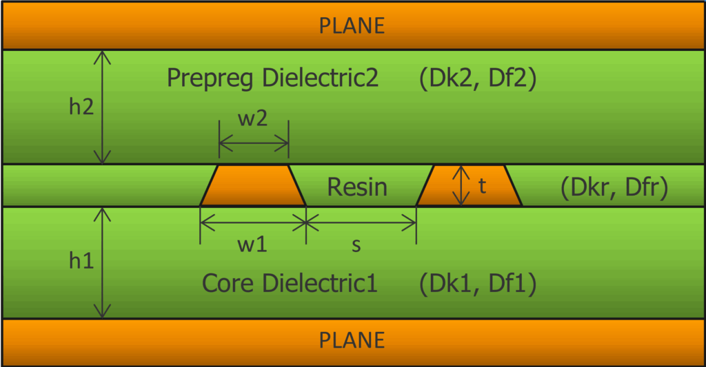
I’m occasionally asked why 0.6 mils (15 μm) is often used to for thickness of half-ounce copper rather than 0.7 mils (18 μm) and similarly why 1.2 mils (30 μm) is often used for 1-oz. copper instead of 1.4 mils (36 μm). If you’re curious about the details or if none of these numbers are familiar to you, here’s a quick primer on the subject. The copper thickness parameter, “t,” in FIGURE 1 shows the thickness we’re interested in here.
Copper weight—why we use ounces
Let’s start the discussion with why weights (ounces) are used to describe thickness.
If someone asked your height and you told them 180 pounds, they’d think you were crazy. However, in electronics, weight is still used as a determinant for copper thickness. Why is that?
The ounce rating has its roots in the gold-foil industry and subsequently for copper’s use in the building industry. It’s based on spreading an ounce of a given metal over one square foot of area. Today’s copper foils for printed-circuit boards are manufactured and sold by weight. The method has persisted in its use for electronic circuits and there’s a good reason for it.
Nominal thickness
Thickness determination of rolled and electro-deposited (ED) copper foil by weight provides far more accuracy than contact-thickness gauges. Since the topography of treated foil varies greatly, and since the density of copper is known, weighing a 1-by-1 foot sheet is the best way to determine the average thickness of a sheet of copper. So formally, the unit that we refer to as “ounces” is actually ounces per square foot. For example, 1-oz. copper weighs one ounce per square foot and is 0.00135 inches or 34 μm thick, nominally, as shown in TABLE 1. Some sources report the nominal thickness of 1-oz. copper at 35 μm, but I’m working off of the IPC numbers here rather than Wikipedia.
| Copper Weight (oz.) | Nominal Thickness | After Fabrication | 90% of Nominal |
| 1/2 oz. | 0.68 mils (17.1 μm) | 0.6 mils (15 μm) | 0.61 mils (15.5 μm) |
| 1 oz. | 1.35 mils (34.3 μm) | 1.2 mils (30 μm) | 1.22 mils (30.9 μm) |
| 2 oz. | 2.7 mils (68.6 μm) | 2.4 mils (61 μm) | 2.43 mils (61.7 μm) |
Go beyond copper thickness.
Explore the relationship between copper roughness and signal integrity. Discover 10 critical things you need to know about copper roughness and its impact on board costs during your stackup design process.

IPC-4562A
You may read other values for these nominal copper thicknesses from other sources, but the manufacturers in the PCB industry are working from IPC-4562A, the “Metal Foil for Printed Board Applications” standard. If your laminate or copper vendor is providing you with different thicknesses, you may want to use this standard—or this article—as a guide for double-checking the numbers they’re providing. To this day, in fact, I see electronic design (EDA) tools using nominal copper thicknesses in their stackup representations rather than the as-fabricated thicknesses.
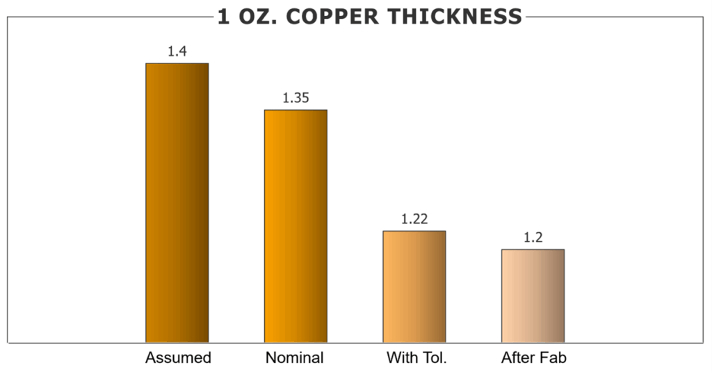
The subject of copper thickness and weight becomes even more interesting when you factor in the tolerances described in IPC-4562A, which specifies that the minimum thickness shall not be below the nominal value in TABLE 1 by more than 10 percent. If you’re a copper manufacturer pushing 2,000-5,000 tons of copper foil out per month and you can keep your volume-production copper weights above 90 percent of the nominal values in TABLE 1, that’s a great way to save some money and that’s in fact what happens in practice. The third column in TABLE 1 shows these 90 percent of nominal values, which are shown graphically for one-ounce copper in FIGURE 2.
After fabrication
After fabrication, including the etching and cleaning processes, the final thickness of these foils will average 0.2 mils (5 microns) thinner than the “assumed” copper thickness (1.4 mils) for one-ounce copper, as shown in FIGURE 2. TABLE 1 shows that half-ounce copper will have a final thickness of about 0.6 mils (15 μm). Your fabricator may have an etching process that differs slightly from these values, but on 95 percent of the stackups I see from fabricators, these are the values they use.
As a side note for comparison, the aluminum foil that most people use for household cooking purposes is about 0.6 mils (15 μm) thick, just like half-ounce copper.
Consequences of using inaccurate copper thicknesses
If you’re looking to calculate bulk resistivity from sheet resistance, sheet thickness is in the denominator and whether you’re getting the copper thickness from an assumed or estimated thickness as opposed to the weight-based methodology noted above, you need to have an understanding of the real values in printed-circuit boards rather than values you might find on Wikipedia, for example.
I often see engineers, designers and EDA tools rounding the above nominal values to 0.7 mils (18 μm), 1.4 mils (36 μm), and 2.8 mils (71 μm). I’m not normally against rounding, but when you’re rounding in the wrong direction, it needs to be questioned.
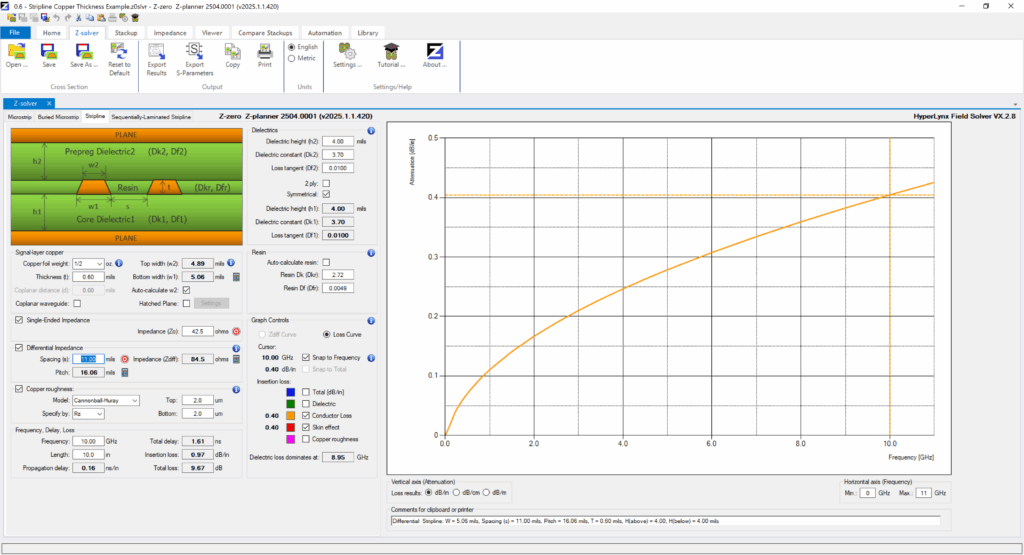
Board thickness, too, will be affected. On a four-layer design, the difference may not be significant, but on a 20-layer design using one-ounce copper throughout and the wrong assumptions, your board thickness will be off by as much as 4 mils. I’m pretty sure the mechanical engineers, if no one else, would appreciate it if PCB designers worked with a sharper pencil. FIGURE 3 shows impedance and skin effect loss at 10 GHz for an 85-ohm example cross section for half-ounce copper using the post-fabrication number.
Conclusion
Truth be told, the difference between using a 0.7 mil copper thickness and the more-correct 0.6 mil thickness isn’t huge, but if you’re tracking millivolts and picoseconds while signaling at multi-gigabit SERDES speeds and taking the time to simulate virtual prototypes using expensive signal-integrity software, it only makes sense to take every form of avoidable uncertainty off the table. Differential impedance will be affected. Signal integrity and crosstalk simulations will be affected. And losses from skin effect will be affected at some level. Why not feed that expensive SI simulator real numbers?