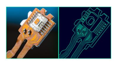
Mastering rigid-flex PCB design: A simplified guide

There is a growing demand for compact, efficient, and versatile printed circuit boards (PCBs). Rigid-flex technology, enabling the creation of boards that can bend and flex without sacrificing performance or reliability, is a crucial solution to meet these demands. However, mastering the design of rigid-flex PCBs presents unique challenges. Whether you’re an experienced designer looking to expand your skills or a newcomer to the field, this guide offers a simplified, structured approach to rigid-flex PCB design.
Differences between rigid and flex PCB design
While there are only a few differences between executing rigid and flex PCB designs in a PCB design tool, these distinctions are crucial for success.
Regional stackups
- Unique stackups for each board region: Each region can have a unique stackup defined by separate board outlines, labeled as either “rigid” or “flex.”
- Master stackup: A master stackup, combining all regional stackups, drives the tool.
Flex-specific layer types
- Special layers: Flex core, cover layer, adhesive, and stiffeners are supported.
- Mask layers: Separate mask layers can be added for each board region, beyond the traditional top and bottom solder masks.
Flex elements in the pad stack
- Pad stack: Includes cover layer openings for through-hole and surface mount device (SMD) pads, and pads defining hole openings in stiffeners.
Bend areas
- Defining bend areas: Bend areas define where and how the flex circuit bends, used in design rule checks (DRC) and 3D design.
Fabrication output
- Communicating design intent: Design intent and regional stackups are conveyed to the board fabricator via Xpedition Layout ODB++ output, the preferred format for flex and flex/rigid designs.
A simple 10-point rigid-flex design process
- Set rigid-flex technology
- Create a master stackup
- Define multiple board outlines
- Assign layers
- Establish route borders
- Create bend areas
- Place and route
- 3D visualization
- Run DRC checks
- Create outputs
By following this structured 10-point process, you can navigate each phase of rigid-flex PCB development with confidence. Whether working with flex-only designs or complex flex-rigid configurations, these principles equip you with the knowledge and skills needed to overcome the challenges of rigid-flex PCB design.
For a comprehensive explanation of the rigid-flex design flow, please download the full whitepaper, Rigid-Flex PCB Design Guidelines. This guide includes “how tos” on all ten steps including creating stackups, defining board outlines, layer assignment, route borders, and more, with clear instructions and illustrations.
Remember, getting the hang of rigid-flex design is a continuous journey. You’ll run into unique situations and chances to innovate as you go. Embrace these challenges, keep learning, and use the tips from this guide to push the limits of your rigid-flex PCB designs.