High density interconnect (HDI) and ultra HDI PCB technologies
In the ever-evolving landscape of printed circuit board (PCB) technologies, high density Interconnect (HDI) and Ultra high density Interconnect (Ultra HDI) stand out as cutting-edge solutions driving innovation across various industries. In a recent podcast, I had a compelling conversation with Anaya Vardya, CEO of American Standard Circuits (ASC), diving deep into the complexities and potential of these advanced technologies.
The growing significance of HDI and Ultra HDI
We explore the growing significance of high density interconnect (HDI) and Ultra HDI technologies, which enable denser component placement and increased signal integrity compared to traditional PCB designs. From consumer electronics to automotive applications, these technologies have a growing impact on the landscape of modern electronics, allowing for smaller, lighter, and more powerful devices.
Challenges in implementing high density interconnect technologies
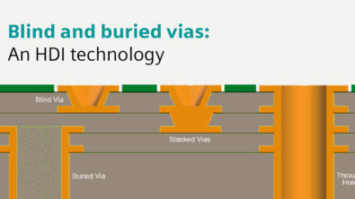
Vardya delves into the challenges that designers encounter when implementing HDI and Ultra HDI technologies. Firstly, he discusses the technical complexities inherent in these advanced technologies, such as achieving ultra-fine line and space dimensions and managing impedance control in high-speed signal routing. Designers must grapple with intricate design rules and manufacturing constraints to ensure the reliability and performance of their PCBs.
Additionally, Vardya addresses the organizational hurdles that often impede the adoption of advanced technologies. Resistance to change within companies, entrenched workflows, and risk aversion can hinder the willingness to embrace new approaches and technologies. Overcoming these internal barriers requires effective communication and leadership to align technological adoption with business objectives and customer needs.
Vardya then highlights the importance of collaboration with fabricators in overcoming manufacturing challenges associated with HDI and Ultra HDI technologies. Designers must engage early and frequently with fabricators to address manufacturability concerns, optimize the design for efficient production, and mitigate the risk of costly rework or delays.
Moreover, Vardya emphasizes the critical role of education in addressing these challenges. Designers need comprehensive resources and training programs that equip them with the knowledge and skills required to master HDI and Ultra HDI technologies effectively. Continuous learning and professional development are essential for staying ahead of emerging trends, evolving standards, and innovative solutions in the fast-paced world of PCB design and manufacturing.
The evolution of ultra high density interconnect
Highlighting the evolution of Ultra HDI technology, Vardya discusses its historical prevalence in chip-scale packaging in Asia and its recent surge of interest in North America. He shares ASC’s successes in achieving ultra-fine line and space dimensions, underscoring the importance of partnership and patience in navigating this frontier of PCB technology.
Insights on high density interconnect and ultra high density interconnect
Throughout the conversation, Vardya offers practical insights and future prospects for designers looking to harness the potential of high-density interconnect and Ultra HDI technologies. By embracing collaboration, education, and a pragmatic approach to technological adoption, designers can unlock new possibilities and stay ahead in an ever-evolving industry landscape. From improving performance and reliability to enabling innovative product designs, HDI and Ultra HDI technologies hold the promise of a brighter and more efficient future for electronics manufacturing.