PCB design best practices: concurrent design
The second PCB design best practice that falls into the engineering productivity and efficiency pillar is concurrent design.
What is concurrent design?
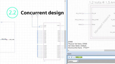
Concurrent design is when multiple engineers can work simultaneously in the same database, but more specifically within the PCB schematic, constraints, and layout. Typical design edits will appear dynamically to all active users within the database, where constraint edits are performed in a controlled and methodical process to mitigate any design rule conflicts that may present themselves while making rule changes within the constraints, on the fly.
What’s not working?
The legacy process is still a serial approach, which is inefficient. It’s inefficient because this approach requires waiting for one task to end before another one begins. Instead of waiting for one user to finish their work and hand it to off to another so they then start their respective tasks, we could be doing tasks in parallel and simultaneously, increasing optimization and team collaboration (less back and forth iterations), which has a much higher potential to shorten engineering design cycle time. This correlates to potentially much shorter project schedules and lower overall cost.
What are the roadblocks?
Internal company culture is one of the biggest roadblocks to mention. This pertains to resistance to methodology change or to buy-in to concurrent engineering. Other typical roadblocks that we’ll see when trying to implement concurrent design practices is that people don’t feel comfortable with others touching the database while they’re working in it. Typically, individuals may not want anybody to modify their work that they have already completed. Many people do not want to have their in-process “work” or in-process “effort level” seen by others because it can feel like you’re being micromanaged while doing your job, which is not the case at all, and leads to resistance and potential roadblocks.”
Another potential roadblock to mention is tool utilization and or feature implementation. Lack of expertise and or experience utilizing the PCB design tool has the potential to amplify resistance to methodology change or prevent the necessary buy-in to concurrent engineering.
Per the legacy methodology, we tend to work in silos, and for many companies, there’s really no incentive to make a change in the process or modify how we do things because we’ve managed to be successful so far with these legacy methodologies still being implemented today.
Best practices: concurrent design
Using advanced capabilities regarding concurrent engineering for schematic and layout efforts is the PCB design best practice. What I mean by this statement, is in the schematic I could have two or three users actively working simultaneously. Basically, I can have two electrical engineers (EEs) or three EEs working in the schematic at the same time. I can also have multiple PCB designers working in the layout at the same time. In either scenario, multi-users can actively be providing effort all at the same time and in the same database.
We also have the capability to have multiple schematics edits taking place in the front end, which is the schematic, and multiple designers in the back end working in the layout, making layout edits at the same time as well. Everyone working simultaneously in one project database at the same time. That’s horsepower when you think about how many man hours you can achieve by attacking your design with multiple users all at one time.
Concurrent design allows you to optimize multidiscipline integration in the database as well as optimize team utilization. The value you’re going to get from this is that you can accelerate design cycle time, reduce development duration and cost, as well as improve design optimization and efficiency. With real time concurrent engineering, you can also enable simultaneous multiuser and multidiscipline contribution
How it works: concurrent design
Working concurrently on a design can accelerate design time and reduce product development cost, since real-time concurrent engineering enables multiple individuals to contribute simultaneously to each task.
Concurrency during a PCB design comes in many forms. The important aspect to being productive, is that engineers and designers on a project team need to be able to work on the aspect of a design that they are assigned to or responsible for, while others in their team are doing the same, respectively. Using Xpedition, engineers and designers can be working together in the schematic, the layout, or both, simultaneously in real time.
Now let’s look at reality and how concurrent engineering has the potential to have huge positive return on investment (ROI) on your project. In the legacy serial approach of engineering, you have one individual working on a specific task within the design process in an eight-hour shift. That individual then produces eight man-hours of effort in his/her working shift, while other team members are waiting to get a hand-off for their chance to work on the database.
On the flip side and when utilizing concurrent engineering, let’s say you have two engineers working on the schematics (front-end) and two PCB designers working on the PCB layout (back-end). That’s a total of four individuals. So, in the same eight hour working shift, we get 32 man-hours of effort (4 x 8). You can see how quickly the numbers divert from one another between the legacy approach vs concurrent engineering, especially when you think about a typical project duration. In general, we typically say, “Time is money”. Concurrent engineering has the highest potential to reduce development time and in turn reduce engineering cost.
To learn more about concurrent design visit our website or watch this video:


