Products
High-speed Wireless PCB Design and Why You Need to be Concerned!
Will the next generation high-speed wireless communication effect you? Most likely, at some point almost everything that contains electronics will incorporate the 5th or higher generation wireless communication. As we move into this new era, the data rate will increase almost 100 fold over our current 4G technology, along with much lower latency rates. This will allow communication between devices like vehicles which allow for self-driving cars. The changes that will occur due to this increased data transfer and ultra-low latency times will dramatically change our lives in ways we can’t even imagine currently due to the flood of new data that will available.
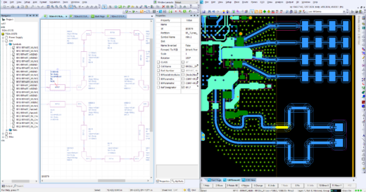
So, why will this next generation of wireless cause you to look at new tools or technology to design our products? Because the frequency range being considered for this 5th generation is 6 to 100 GHz. At these frequencies the RF elements in your design are much more complex and in most cases will require simulation using a 3D solver. Along with that come other design challenges most PCB design tools do not include.

These would include:
- Complex via stitching
- Cavities
- Integration with RF simulation applications
- Complex trace geometry
- Rules specific to RF structures


