You’re in the planning stages of your next design with requirements for a DDR channel with 4 chips and a 2 SerDes channels along with other supporting circuitry. Based on past projects you create a timeline for the electrical design and PCB layout.
When presented to management they are not happy with the schedule and ask you to shave 2 weeks to meet release goals due to market pressures. You don’t have additional resources you can use to complete the design in less time so you look at other options. The best solution you’ve found is to use the routing automation capability of your PCB tool instead of routing the entire design by hand like all previous projects.
Design Rules
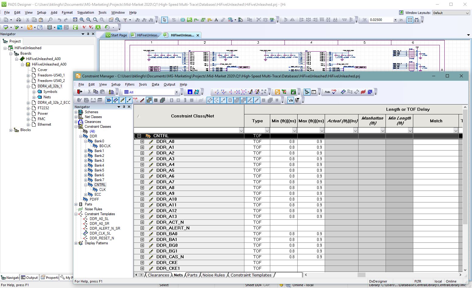
Figure 1 – Schematic CES
These are the backbone of creating a PCB design to achieve first pass success, meet electrical requirements, and produce a high quality product. Even a basic PCB needs some kind of rules; trace widths, copper to copper spacing, component spacing, etc. As we work on designing the schematic we will create most our rules via the Constraint Editor System (CES) Figure 1. To properly use automation later or even make hand routing easier we need to create Constraint Classes were are timing/length matching rules will be defined along with differential pairs, topology, cross-talk, and other electrical rules.
For our DDR circuit we will create a DDR Constraint Class with sub-classes for Data banks 0 to 7 and Address\Control. After we place components we will update the timing rules for each sub-class. For copper-to-copper clearance rules we do something similar by creating a Net Class for DDR with sub-classes for Data banks 0 to 7 and Address/Control. In addition to clearance rules we can also define what layers each group can be routed on and the trace width for those layers based on calculations we did using the stack-up editor in CES.
Routing Automation
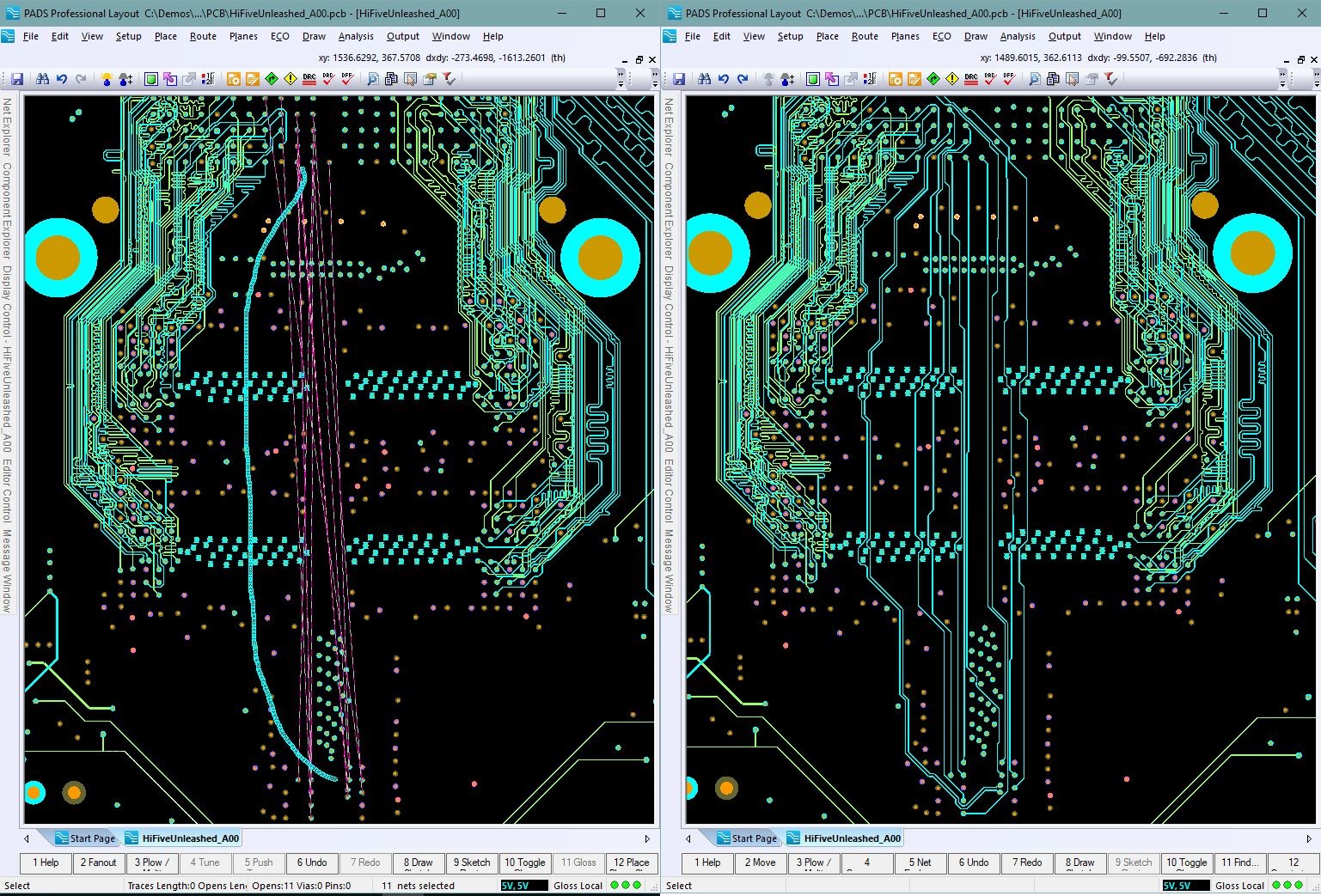
Figure 2 – Sketch Routing
Autorouting is no longer a push button and see what happens process. Today’s technology uses a fully guided process giving you the power to decide where traces will be placed but the tool do all the routing. With our rules defined already from the schematic and part placement completed we move onto routing. First we’ll attack the DDR circuit Figure 2. Seeing this is the first time we’ve decide to use Sketch routing for a complex part of a design we’ll run a few test routes. After a few attempts we quickly discover how powerful and simple this technology is to use. It also comes to our surprise the quality of the routing and how similar it is to hand routing. In less than an hour we are able to completely route our DDR circuit to 100% completion.
Timing Rules
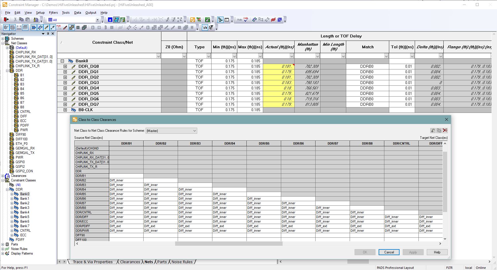
figure 3 – CES Matching Rules
However, we are not done. To meet our timing goals for clocks, data, and control we need to match sections of the DDR circuit. Planning for this ahead of time we already have most the proper constraints defined. The only adjustment we need to make is for length or time of flight (TOF) based on our placement. Using the same CES system we did from the schematic we will adjust our length rules based on time Figure 3. Seeing we have intimate detail of the DDR circuit it’s much easier to stay with timing constraints instead of converting to physical length. Plus the calculated timing values reported will include delays through vias given this data has been added.
Trace Tuning
Too many designers today are still using the tried and true hand tuning methods. It works, it’s accurate, but it’s time consuming. We’ll start tuning traces by groups using our Net Explorer which has all the Class and Constraint Classes (groups of nets with electrical rules like time of flight) we defined in CES. This greatly simplifies the process of finding and selecting objects to be worked on. Before we start tuning we can define global settings for the tuning objects that the automation will create.
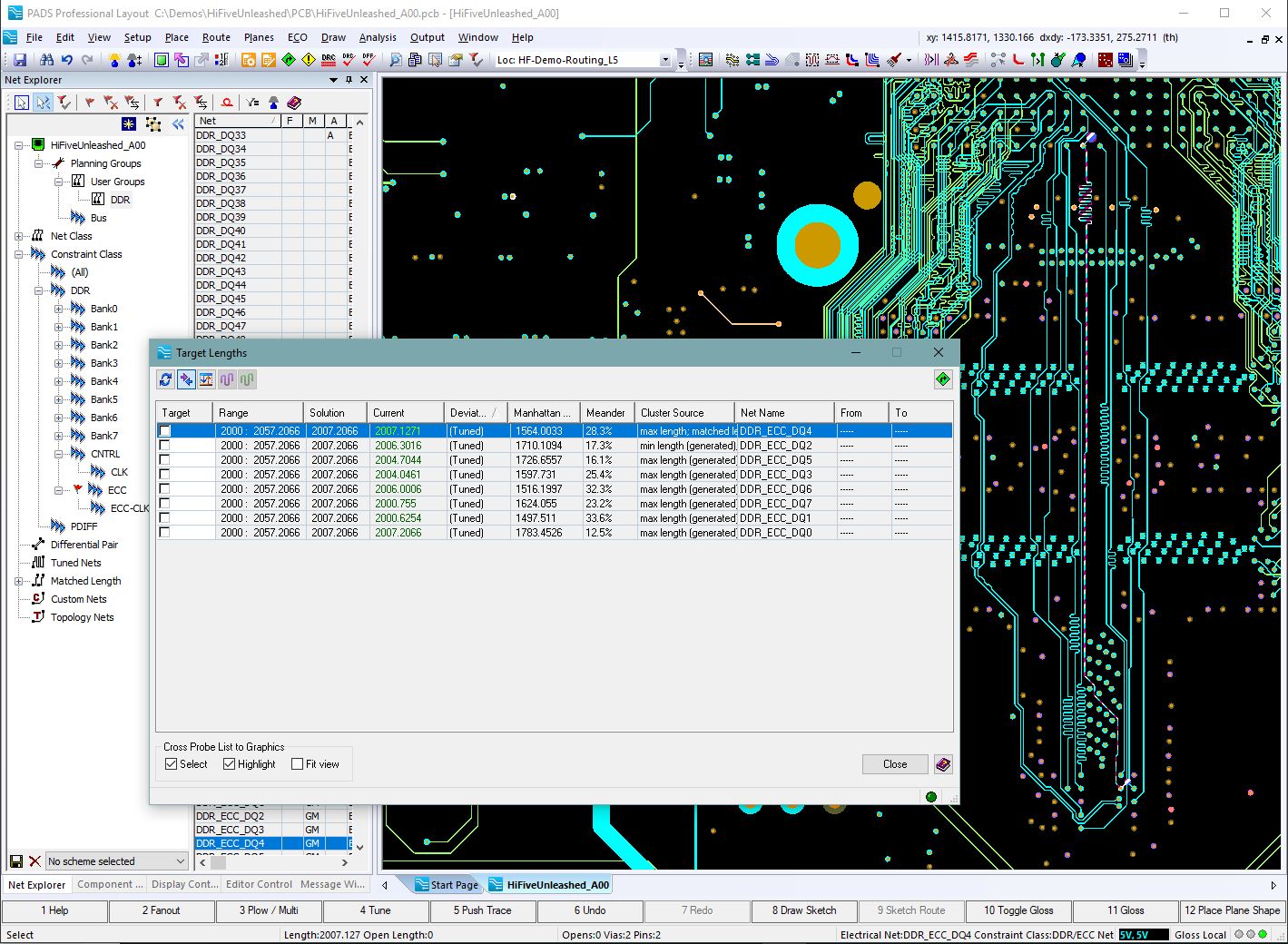
Figure 4 – Multi-trace High-speed Tuning
Items such as: Min\Max height for serpentines, regular or irregular pattern, miter ratio for direction changes for arcs or 45’s, saw tooth settings for differential pair tuning. Select a group in Net Explorer DDR>Bank0, right click in the work-space and choose tune. It’s that simple. With-in a few seconds most or all the selected nets will be tuned based on the TOF rules we defined in CES.
If for some reason 1 or 2 traces do not tune its most likely due to space. Using trace push-n-shove we can create some added space and tune again. For a quick check to see if all nets are matched or how much any trace is out of tolerance we can use the Target Length function. This function can be used to choose a net to tune to and also start the tuning process. Its main function is to get quick feedback on the length of those nets selected and if not matched how much each is out of tolerance. Tuning features are added as an object so if more space needs to be added you can select a tuning object and quickly move it without losing any of its integrity. With our first group completely matched in a few minutes we can move on to each of the Data banks and finish with Address and Control. 60 to 90 minutes later we are done tuning all our nets.
With a little bit of added work upfront creating new rules for length matching via additional Classes, Constraint Classes, and spacing rules. We can use automation existing today that’s simple to learn, extremely powerful letting you control where objects are placed, and provides results with similar quality to routing by hand. However, with automation we can take part of a design that would have required 30 – 40 hours and reduce it to 8 hours or less.
To learn more about PADS Professional Multi-Trace tuning technology, watch this video with a full demonstration of the power and productivity gains you can realize as you upgrade and get more with PADS Professional!
December 8, 2022In our second episode of the Printed Circuit Podcast, we talk about existing infrastructure within organizations and why it’s adding...
This article first appeared on the Siemens Digital Industries Software blog at https://blogs.sw.siemens.com/electronic-systems-design/2019/12/16/real-world-example-of-how-pcb-routing-automation-reduces-design-time/