Highlights from SPIE – Successes and advancements over the past year
By Gandharv Bhatara – Mentor, A Siemens Business
At the 43rd SPIE Advanced Lithography conference in San Jose that ran from February 26th to March 1st, Mentor continued to demonstrate its leadership in computational lithography with 22 papers and posters, majority of which are written in partnership with several leading-edge foundries, that demonstrates the widespread usage and application of the Calibre tools at these various foundries.
Mentor continues to invest and innovate in both DUV (immersion lithography and multiple patterning) as well as in EUV. In both these areas, challenges persist that need novel solutions. More specifically the focus continues to be in the following area:
- Optical proximity correction (OPC) and resolution enhancement technology (RET) solutions to understand process limits and expand process margins/windows
- Applications, flows and methodologies that allow foundries to increase their productivity thereby reducing development cycle times, complexity, and costs
- Creating fast, scalable production solutions that minimize the post-tapeout flow turnaround time
In that context, I’d like to highlight a couple of advances that we have made in the past year that were presented in this year’s SPIE.
Dealing with the Memory OPC Challenge
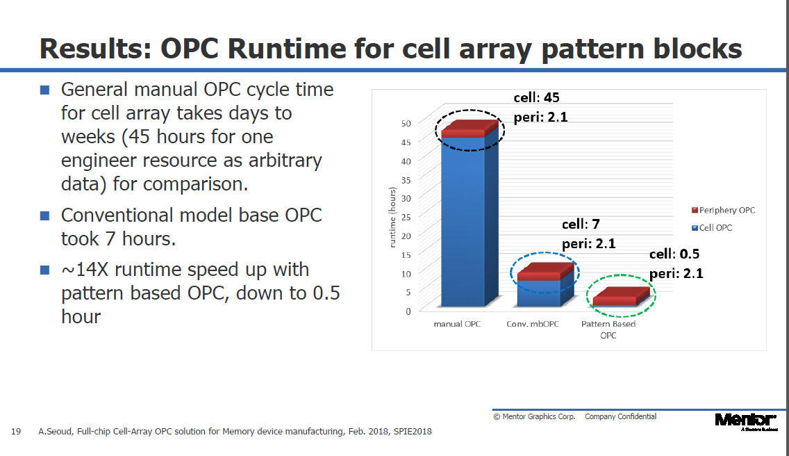
Typically, OPC for memory-style designs, i.e. large blocks of repeating arrays/structures, is done manually. The problem with this approach is that it is a slow and iterative process that can take weeks to implement and is prone to human error (See Figure 1)

This has been an area that has been ripe for innovation for a while but solutions have been hard to come by, until now. The main challenge being that any solution in to address this problem must satisfy the following criteria:
- Consistency: 100% consistency for post-OPC shapes (0nm inconsistency)
- Turn Around Time: Competitive runtime of full chip OPC + SRAF (< 12 hrs.)
- Design Capabilities: Can handle advanced designs
- Automation: Full automated flow (no manual intervention)
In Calibre, we have invented a new fully-automated pattern matching technique that delivers on all of the above criteria (See Figures 2 and 3). For more details on this approach, refer the presentation that was done with SK Hynix “Model-based cell-array OPC for productivity improvement in memory fabrication” by Seoud et al.

Another challenge, which isn’t specific to memory style designs, but is equally important in resolving so as to get an optimal memory flow, is in the area of SRAF (sub-resolution assist features) placement.
The industry has struggled to find the optimal approach that allows one the process window they need and can be done in a way that’s computationally feasible. Rule-based approaches have been around for a while and they guarantee perfect consistency but can be hard to implement. Model-based approaches are easy to implement but can be limited by their consistency. The optimal solution is a hybrid approach that takes the best of both rule-based and model-based insertion schemes.
We invented a new technique that allows one to reduce recipe development time using this hybrid approach as well as making it very easy for an engineer to build the recipe. We do this with a novel automated Model Assisted Template Extraction (MATE) approach. With this approach an engineer can now do SRAF recipe development in hours as opposed to days or weeks. This approach has become the industry standard at the advanced process nodes. The value of this approach is also demonstrated for the memory OPC flow (that have stringent consistency requirements that precludes model-based approaches) in this publication: “Model-assisted template extraction application to contact hole patterns in high-end flash memory device fabrication” by Seoud et al.
Meeting the EUV Challenges
While Mentor has had “working” computational lithography solutions to EUV for several years in use by several leading foundries for EUV development, the entire EUV patterning process (scanner, materials, resist, process integration) continues to evolve. This presents new challenges and new opportunities. At this year’s SPIE we had 5 publications that talked about some of the newer trends and activities in EUV computational lithography and in this blog I will address two specific areas of interest.
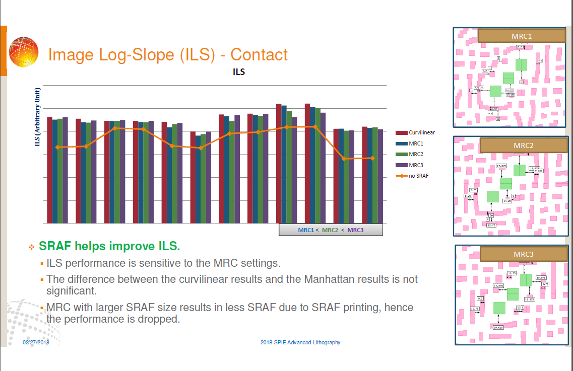
The first challenge deals with the question of whether SRAFs are needed or help improve the process margin with EUV and if so, what would be an ideal approach? EUV RET optimization for next generation designs involves co-optimization and many complicated trade-offs. In a joint effort with GLOBALFOUNDRIES and IMEC, we were able to ascertain that with powerful optimization tools, such as Inverse Lithography Techniques, and careful balancing of requirements, SRAFs can provide an enabling element to achieve required process latitudes (see Figure 4). SRAFs can help improve image quality and process window, and mitigate image shift through focus (see Figure 5). For more details refer to the following publication: “SRAF requirements, relevance, and impact on EUV lithography for next-generation beyond 7nm” by Guo et al.

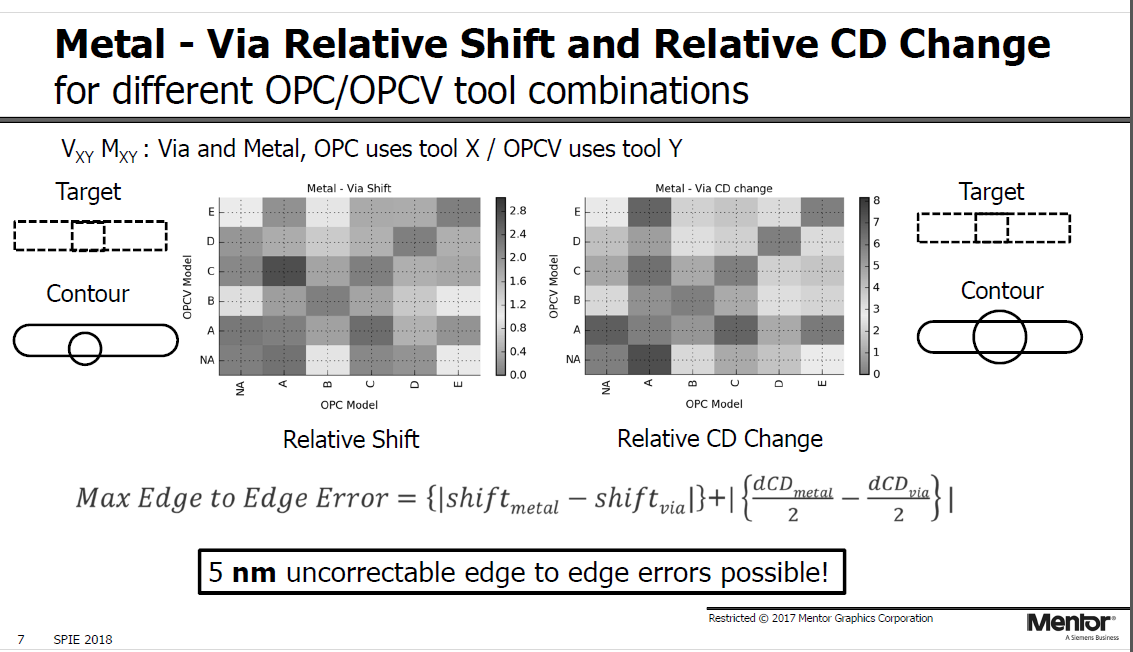
The second challenge deals with handling the impact of aberrations in EUV lithography. In previous works, we have described how EUV scanner aberrations can be adequately simulated and corrected in OPC across the slit to deliver excellent edge placement control. The problem is that the level of aberration variability from tool to tool is currently quite significant and leads to uncorrectable edge placement errors if OPC is done using one tool while exposure happens on a different tool. This means that the current and near-term anticipated aberrations levels on EUV scanners implies very significant edge control challenges (see Figure 6).

For a fleet of EUV scanners in manufacturing, when considering the different combinations of aberrations referenced in OPC and aberrations referenced in verification, across two layers with critical inter-layer edge placements, the number of possible combinations is substantial, yet certain combinations will yield better lithographic results than others. Computational lithography can be a very powerful tool for assessing these combinations for manufacturing use. We have demonstrated a clear advantage of using dedicated OPC models with tool-specific aberration correction. Without such dedication, up to 5 nm of uncorrectable relative edge placement errors can be realized (Figure 7). For more details, refer to the following publication “Impact of aberrations in EUV lithography: metal to via edge placement control” by Yin et al.
Mentor is creating innovative solutions for DUV and EUV lithography. Advances in OPC and RET are expanding the process margins/windows and new applications, flows, and methodologies increase foundry productivity. Mentor continues to partner with semiconductor companies and foundries to improve the quality, cost, and turnaround time of the post-tapeout flow.