What does physical verification need today?
By Juan Rey – Mentor, A Siemens Business

Physical verification has come a long way from its humble beginnings of doing a few Boolean operations on geometrical shapes and measurements to compare against a small set of dimensions to determine if a design could be manufactured or not.
In fact, the combined growth in complexity of integrated circuits and of the semiconductor manufacturing processes resulted in computational requirements that early on outpaced the computational power delivered by Moore’s law, and show no sign of slowing down.
Where did that computational complexity come from? Well, to start with, the total number of transistors on a die of a given area doubles approximately every two years (Figure 1). That growth translates directly into a corresponding growth in the number of verification operations.
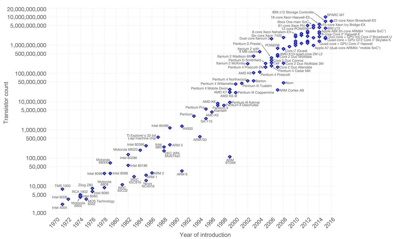
Figure 1. Growth in number of transistors over microprocessor generations.
In addition, when approaching the limits of the semiconductor processes’ ability to faithfully reproduce the structures created by the designer, most notably (but not only) due to the looming resolution limit of the photolithography process, the number of operations in the design rule manual has been growing exponentially (Figure 2).
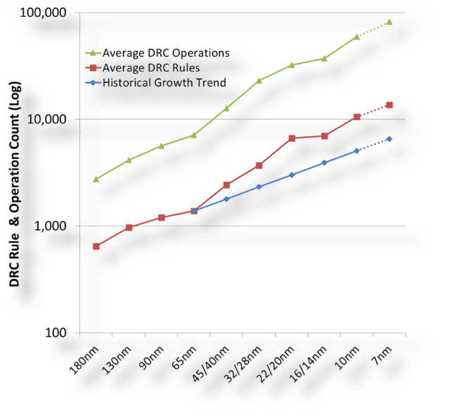
Figure 2. Growth in design rules and rule operations.
Unfortunately, just “verifying” the design does not suffice to yield a circuit that functions as intended (or at all). It is always necessary to modify the design to compensate for process limitations, such as adding sub-resolution assist features, adding “dummy” features to produce layers of more uniform density, splitting a layer in multiple layers to enable multi-patterning, or finding problematic patterns and replacing them for alternative ones that are “known good” from a manufacturability point of view.
One of the often-overlooked aspects of these activities is the need for physical models that accurately capture the results of corresponding semiconductor processes and that can be applied at full chip level while delivering results in customer-acceptable turnaround times. This is, for example, critical for activities that check the lithographic manufacturability of the design (as when using the Calibre® LFD™ tool to determine the “litho friendliness” of a design) or evaluate the layout density impact on thickness variation during a chemical manufacturing process. Figure 3 shows the many types of verification activities used at advanced nodes.
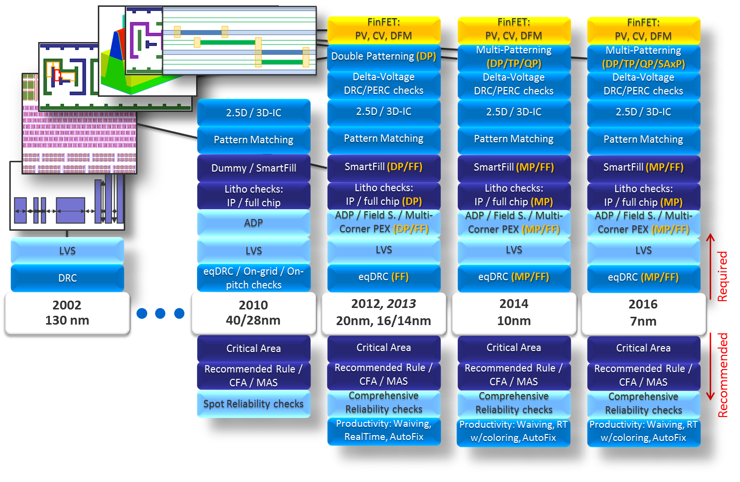
Figure 3. Growth in complexity and number of verification activities.
To deliver verification toolsets such as the Mentor® Calibre nm Platform, a combination of physics-based knowledge, computer science, and engineering skills is required. The physics-based knowledge is critical for the creation and development of the necessary models, while the software engineering skills are essential to accomplishing full chip-level verification/diagnostic and modifications of the layout in overnight turnaround times.
But going back to the main topic, “What does physical verification need today?”
First, it requires a toolset that encapsulates all the physico-chemical aspects of the semiconductor process to deliver sub-nanometer accuracy verification and layout modification. For example, it must be able to consider key effects of the chemical mechanical polishing (CMP) process, as well as the aspects related to the patterning process, such as modeling of the photoresist exposure effects through the complete process window (through exposure dose and focus) and associated photoresist development (Figure 4).
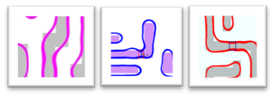
Figure 4. Predicting actual lithographic results and potential lithographic “hotspots” is an essential internal step in the Calibre LFD process.
Second, to compensate for the gap between the computational power delivered by Moore’s law and the additional complexity of the “physical verification activity” requires leading-edge computer science and software engineering skills to provide scalability through both shared memory processors and distributed computing, as well as constant improvements on algorithms for single processor operations.
In other words, the “carefree” times when more complexity due to the larger number of polygons per chip was compensated for by the increase in processing speed of the most recent microprocessor generation are long gone, as that added complexity due to manufacturing process limitations can now only be mitigated by smarter processing in general, and more specifically by parallel processing. In fact, this need was only exacerbated by the failure to increase processing speed a few generations ago, and the result was the move from single-core to many-core processor architectures.
While every EDA vendor chooses its own path to product improvement, at Mentor we continuously evaluate and refine the functionality in the Calibre suite to ensure ongoing customer success and productivity, as well as continuity in the customer experience. Figure 5 shows the typical rate of runtime improvements that Calibre tool optimizations can deliver. In this case, runtimes for the Calibre nmDRC tool were measured across several tool releases for over 20 large SoC designs targeting processes at or below 28nm. The runtimes were averaged to illustrate the expected runtime improvements for typical designs.
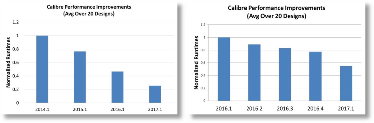
Figure 5. Not only has Calibre performance improved significantly year over year, but it continuously improves from release to release.
The results of Calibre scalability improvements are shown in Figure 6. In this graph, you can see the runtime reduction achieved for the same design simply by using a larger number of processors.
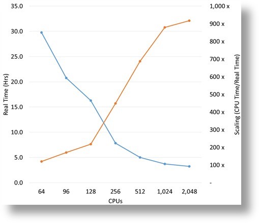
Figure 6. Calibre productivity optimizations are further enhanced by expanding the software’s ability to access a large number of processors, with a resulting decrease in runtimes.
In summary, physical verification today needs many things from EDA vendors to ensure customer success: expanded layout analysis and fixing capabilities, accurate physical models that reflect and predict process effects, optimized tool functionality that performs as efficiently as possible, and optimized hardware usage models that enable users to maximize the use of their hardware resources. Because the Calibre nm Platform is continuously maintained and enhanced to ensure it delivers on these expectations, IC designers can rest assured that their designs can be comprehensively verified in acceptable turnaround times, even for the most advanced technology nodes.


Comments
Leave a Reply
You must be logged in to post a comment.
Excellent! Fig 1 alone is worth visiting this page!