Self-Aligned Double Patterning, Part One
By David Abercrombie, Mentor Graphics
A walk-through of the SADP process for success.
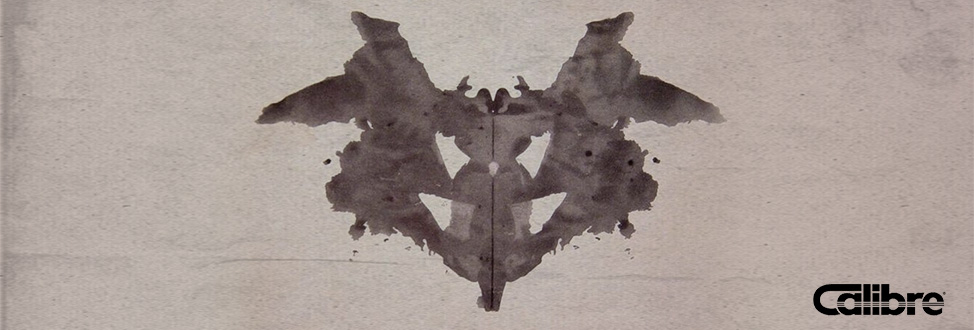
I’m sure most of you have seen a Rorschach test ink blot (Figure 1). Psychiatrists ask the subjects to tell them what they “see” in the ink blot. The answers are used to characterize the respondent’s personality and emotional functioning. I am never sure if I would feel more uncertain being the psychiatrist asking the question, or the subject trying to decide what to say, given there are no “wrong” answers.
Figure 1: Rorschach ink blot. What do you see?
Why am I talking about ink blots? Because I want to discuss one of the newer multi-patterning techniques, most commonly called self-aligned double patterning (SADP), although it is sometimes referred to as sidewall-assisted double patterning. See, already we have two correct answers for the same acronym! In any event, SADP can seem an awful lot like an ink blot—hard to visualize. Let’s explore that thought…
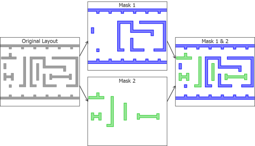
SADP is similar to the litho-etch-litho-etch (LELE) double patterning (DP) you’re all coming to grips with in 20/16/14nm technologies, in that it uses two masks to define the final pattern on the wafer. However, that’s the ONLY thing these two technologies have in common. One of the comforting things about LELE DP is that the two masks are each essentially a copy of part of the original drawn layout. When you look at them together, they look identical to the original layout (Figure 2). If someone asked you what you “saw” in the two mask patterns, you could easily and intuitively describe the original layout.
Figure 2: LELE DP masks compared to the original drawn layout.
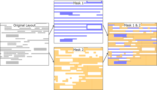
With SADP, this comforting situation evaporates, and the feeling that you are looking at an ink blot takes over (Figure 3). The two masks used to form the final mask shapes have only minor similarities to the original drawn layout, and the translation from the mask data to the original design and vice versa is definitely NOT intuitive.
Figure 3: SADP masks compared to the original drawn layout.
Looking at the mask layers, especially individually, you will probably have a difficult time trying to “see” how they relate to the original layout. The key is to understand the rather unique process that is used to construct the shapes on the wafer using these masks.
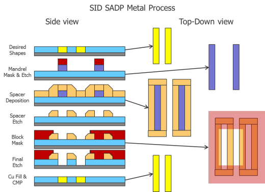
While there are a couple of SADP processes, the version I’ll use is called spacer is dielectric (SID). The steps in the SID SADP process are shown in Figure 4. To help you visualize what’s happening on the wafer, the diagrams on the left show cross-sectional views, and the diagrams on the right show the top-down view of the same step.
Figure 4: SID SADP Metal Process.
The first diagram is the desired end result—in this case, two short trenches in oxide filled with copper for metal interconnect. As with LELE DP, you cannot print these two shapes this closely on a single mask, so one of the two shapes is assigned to the first mask, called the “mandrel” mask.
Unlike LELE DP, the next step is to modify the shape (lengthening it on each end) and add a new shape that was not on the original layout (in this case, another line on the far side of the second shape not assigned to this mask). The mandrel mask is used to pattern a hard mask layer that is then covered with a new deposited layer.
This deposited layer is then etched to leave residuals on each side of the hard mask. These residuals that encircle the hard mask shapes are called spacers. Once the original hard mask is removed, you can see that the spacers essentially define the spaces around the original intended shapes. This step is where the process gets the name SID—the spacers define the spaces between minimum-spaced shapes. You had to add the additional shape on the other side of the second original shape to define the spacer for the other side of that second shape.
The obvious issue is that the spacers don’t block off all the areas of the layout that don’t need trenches. This is where the second mask comes in. Unlike LELE DP, this second mask does not contain the rest of the original shapes. It is more of a wide area coverage mask that protects all the other locations that don’t need trenches. The combination of the two masks used in conjunction with the spacer deposition and etch processes produces the desired final set of trenches on the wafer.
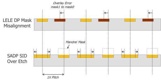
The key to the SADP approach is that the pitch split is achieved using the spacers, instead of aligning one mask to another like you do in LELE DP. This technique is the primary advantage of the SADP process over LELE DP. As shown in Figure 5, LELE DP is prone to misalignment between adjacent shapes from each mask, because there is only so much control the foundry can maintain over the alignment of one mask step to another. In SADP, the lines are inherently aligned because the two shapes are made from the one process (hence the term “self-aligned”). The most difficult process issue in SADP is controlling the etch bias on the spacers. As shown in the example, over-etching of the spacers makes them smaller, creating a width bias between adjacent shapes on the wafer.
Figure 5: Comparison of process control issues between LELE DP and SADP.
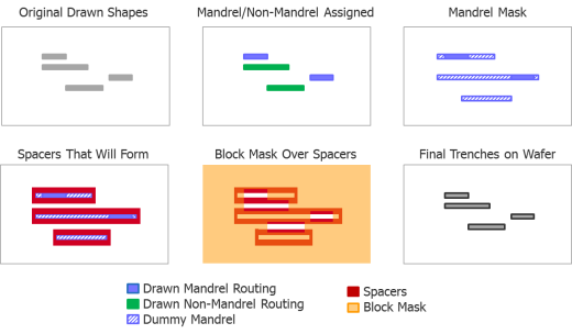
Despite its process advantages in alignment control, SADP is certainly not as easy to comprehend from a design layout standpoint. I’ll give you one more example in Figure 6, shown in a slightly different way, to help you better understand how the original shapes are decomposed into the mandrel and block masks to produce the final shapes on the wafer. Again, the original shapes go through an initial split assignment to determine which shapes will be on the mandrel mask. This division is very similar to what happens when decomposing a design in LELE DP, but the non-mandrel shapes are not placed on a second mask. The mandrel-assigned shapes must be modified (as shown in the mandrel mask box), which includes extending them and adding the additional shapes to make sure spacers will form where they are needed. The fourth box shows how the spacers form around the mandrel mask-defined hard mask. The block mask is then overlaid to expose the desired final trench shapes to the final etch, while protecting everything else on the wafer.
Figure 6: SID SADP layer decomposition.
SADP is certainly not an easy topic to grasp initially. Spend some time with the pictures and explanations, and hopefully, we’ll all begin to see the same images in the ink blots!
Author
David Abercrombie is the advanced physical verification methodology program manager at Mentor Graphics.
This article was originally published on www.semiengineering.com
