Shaping the future of semiconductors with the digital twin – Podcast Transcript
Bringing a new chip design to market is not simply a matter of designing the chip then sending it to be fabricated. Building fabs is, itself, a costly and highly complex process and, even once that is completed, it will still take further time to dial in the chip fabrication process to achieve good yields. All these factors contribute to the costs, risks and challenges associated with bringing new, cutting-edge chip designs to market. So, across the chip design process, adopting the latest in digital technology isn’t just a benefit – it’s a imperative.
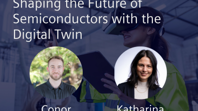
In a recent podcast, host Conor Peick is joined by Katherina Westrich, Global VP of Electronics and Semiconductors at Siemens, to explore how the needs of the semiconductor industry can be served by the increasing adoption of digital twin and artificial intelligence technologies and how that will shape the industry going forward.
Listen to the full episode here or keep reading for a transcript of that conversation.
Conor Peick:
Welcome to the Future Ready Podcast from Siemens. I’m Conor Peick and I’m a marketing writer at Siemens as well as one of a few hosts that you will find on the Future Ready Podcast feed. Today we are happy to have Kathernia Westrich back on the show to talk about electronics and semiconductors. In our last episode together we covered some of the stresses on the industry right now like memory demand and the rise of artificial intelligence. And today we’re going to begin to explore how the industry can transform to meet future challenges and adopt new technologies and how this all affects the construction of new fabs to produce more chips in the future. Thanks so much for joining us and hope you enjoy the discussion. Given this changing paradigm, how do you think the industry needs to transform to meet this evolving paradigm of software-defined, AI-powered, and obviously all enabled by silicon, as you mentioned?
Katherina Westrich:
Yes, I think that it’s very key that we use the digital twin across basically all the different elements of the value chain, really from the sign, but all the way through to building a fab, but then also in the actual operation. This means we have kind of a closed loop approach between the real and the digital world and look at the virtual representation of products or even the whole production, including performance. And with that, we can efficiency, tackle complexities and also boost innovation. I think that’s key and that requires also a certain openness to share data across ecosystem. I think that’s still a challenge in the industry because everyone is very much concerned for a reason that IP might be going lost or someone is risking its IP. And I think this is something where we need to find ways on how we can share in between the different players without harming any IP to really leverage the full potential of technology which is out there.
Conor Peick:
It’s a fascinating balance, I suppose you could say. essentially trying to crowdsource maybe better information, better innovation without exposing your IP to obviously then create a lot of damage for your business if a competitor was able to design exactly to beat you or whatever. It is this kind of fascinating balance between security and openness to spur greater innovation. So I would love to take a quick maybe not a detour, but just to dive a little bit deeper on the concept of the digital twin in semiconductor in particular, because given the complexity of semiconductor devices, billions of transistors on a single chip, obviously we’ve been relying on digital tools for a long time now. I would love to get your thoughts on maybe how you see in semiconductor design, maybe How can they continue to embrace digital twin concepts, digital twin technology to keep finding new advantages, new edges, and to optimize further?
Katherina Westrich:
Yeah, maybe probably if you ask a design engineer in the electronics and automation space, they would say, well, we were probably the first ones. working with digital twins. So this is nothing new for us in this regard. And I think the design phase is very decisive because most of the decisions which you make need to be driven right there. Is it system performance? Is it chip performance? including energy efficiency or also designer piece, or if you look to circularity, for example, does the trip need to go in the second life? Just to name a few, I think that’s very relevant because Most of the people I think forget how important this first phase is actually to then make sure that actually things go the way they should go. But what I’ve talked about earlier, also what I told you in terms of talent shortage and also higher engineering effort, we believe that AI can be an answer also to help in this regard. And that’s why we have built a very comprehensive and generative genetic AI system for semiconductor and PCB design to enhance basically productivity and also accelerate innovation and to speed up also time to market. So I think that’s very critical. And to give you the concrete example is design verification with Questa One. And there we are able basically about depends basically on the application, 10 to 100 times reduction of manual test and we can six times faster simulate. And that’s not only, you know, a statement which we are using, but also MediaTek, our customer is confirming that reduction in engineering time and debugging. And I think these are great examples how AI today is already being used specifically in the design phase to optimize going further.
Conor Peick:
It’s kind of serving maybe a dual purpose of it can help speed up simulations, but also help reduce manual tasks. And with test or verification, I know also sort of algorithmic methods have long been in use to help explore the design space and try and find corner cases. Do you think AI is going to help accelerate that as well?
Katherina Westrich:
Yeah, sure. And I think especially if you look on how expensive also design and verification and the long time periods are, So all of this can be improved with the support of AI. And we will see going forward more and more application of AI also in the design phase, what we are already seeing. I mean, it’s just one example. I could probably give 5 to 10 examples more of what we are already doing. So I think that’s where we already see that it’s real and that we are not just talking about AI as a buzzword, that we are really integrating AI in our tools and that it’s helping already to create value for our customers.
Conor Peick:
As we kind of move forward, you had mentioned the manufacturing side earlier, and I’d like to move on to that now. And obviously, building a semiconductor fab is a pretty massive capital expenditure. It involves a lot of money. But I would love to know, given that expenditure, what decisions do you think leaders are making right now? What are they trying to do to reduce their risk and reduce the time to yield, ramp up production faster? How do you think they’re approaching that?
Katherina Westrich:
There is, I would say, no easy answer to this because it’s dependent on so many different factors from regional factors, geopolitics. technology trends which are all heavily influencing a successful ramp up but maybe to make it concrete let’s take a look at Taiwan I mean they have established over decades a whole ecosystem which enables them to have a really fast ramp up and this is not something you can easily copy and and that’s the benchmark I think right now where everyone is basically competing against but on the other side it’s also not only about I mean, I touched earlier shortly on the dynamics, which we see in the memory chips environment. And memory is usually a very cyclic business. So we expect now a supercycle, but the leaders also need to be careful and manage that, that they don’t sit after a supercycle on overcapacity. So I think these are things which also need to be considered and obviously the topic of integrating new technology like digital twin AI to optimize not only on construction, but then also on the production side is something which is relevant and which we are also doing ourselves. So we build our factories completely digital native, meaning for example, right now, if we look to our factory in Singapore, which is not even built yet, we have a complete virtual model of that factory and can look at material flow, operations, staffing, logistics to identify bottlenecks before we actually have them in the real factory. And I think that’s a strong take where also the semiconductor industry can benefit a lot from and also then with regards to that improve basically time to market. But before we start applying such technologies like digital twin AI, I think it’s also important to state that we need a strong backbone, like a strong data backbone. Because if you have very scattered data around your company and take that as kind of single source of truth and then just apply AI or digital twin, which needs high quality data and also computing power, you might be on the AI side, get garbage in, garbage And on the virtual twin side, maybe there are really not enough computing power to actually run high end simulations. So what we usually do is that we are also using our PLM system, for example, as one key data backbone and then also other several integration layers to make sure we can apply this technology in the right way. And just to give you a stat around that, so 60% of companies in the semiconductor sphere use six or more systems to store or access their product lifecycle management data. And that’s a key challenge because then you have this scattered data around companies. So this is something which you can help with if you have one PLM system which is doing that for you and kind of connecting the different steps from design then also to the production side. And I think, it’s key if you look to time to market to leverage new technologies to have the competitive edge. And there we can, of course, help also with our automation portfolio where we are also applying more and more AI to it.
Conor Peick:
You know, this issue of data silos and all the different data systems that most companies have, you know, I’ve been working on a series in pharmaceutical and life sciences, and you hear a very similar story of, these companies, they have lots of data available. It’s just scattered around, right? Yeah, it’s fascinating to look at how to really apply AI, you have to have a solid data foundation. But I know that there are some applications where AI maybe can help you get a hold of what those data sources are. I don’t know, a little bit of chicken and the egg, right? The classic conundrum. Going back to talking about this question of the expensive fabs and ramp up. Is there a distinction that you make between the ramp up of a new fab entirely? And then are there different decisions that need to be made when you’re thinking about the ramp up of a new chip design? Because obviously that’s maybe a similar process, but different than building a facility.
Katherina Westrich:
Yeah, sure. I think this is completely different, but also somehow interlinks. You know, if there is a new chip design, you know, how are you integrating that also then in your fab, so to say? I think that’s something which is somehow also connected to a certain extent that you make sure also production processes are fitting then also the needs of the design you’re having. I mean, that’s also where you say, for example, if you don’t have your own fabrication, then you give basically the design also to the foundry that they produce it in a way for you and that means also certain adaptation time to make sure that you get basically the yield and the output you need. So I think there is certain connections, but there is also a certain differentiation, obviously to say, Okay, I introduce a new design, and then also to build up a complete greenfield fab, right?
Conor Peick:
Okay, so then how do you think we can help companies? achieve this accelerated time to market, faster ramp up and reach that yield quicker.
Katherina Westrich:
Yeah, I think, I mean, if you apply, for example, I’ll take an example, the topic of facility monitoring control system, where Siemens is a leading player, but this is, for example, totally hidden. So basically beneath the fab lies the sub fab or basement, depending on how you would like to call it. And that’s That’s a network of systems which is often overlooked from the outside because no one basically sees it. But that’s actually what powers the clean room at the end and also the clean room’s position, so to say. These systems make sure, for example, that the clean room is running on constant temperature, on constant humidity. There are abatement systems which neutralize, for example, toxic gases, chillers, cool, ultrasensitive tools, gas and chemical cabinets. regulate the flow of essential materials. So also the whole energy infrastructure is there and these systems are a combination of hardware and software for example. And traditional automation engineering for such complex systems with I would say probably about 30,000 plus rather assets in facility monitoring control systems is very tedious, error prone and also time consuming. But what we are now being able also to do with AI is that you can automatically create, for example, a controller or human machine interface code and that you have basically kind of a 24/7 expert which can guide engineers or maybe if you don’t have engineers anymore, maybe not so educated people in the field that they guide basically that are guided by AI to fulfill the complex tasks and the engineering platform functionalities which are needed. And that’s a massive increase in efficiency and drastically reduces the engineering effort and at the same time also increases the quality because It’s less error-prone, so to say, and that has a big increase also on the quality in this regard.
Conor Peick:
So that is super cool. It’s almost like using big Lego blocks to make functionality requirements, which then have their own underbelly of immense customization to make them fit together the right way. Really fascinating. So again, Katharine, it’s so great talking with you and I already have more questions to ask you for our next conversation, which will hopefully be soon. And thank you so much to the audience as well for joining us. We’re always working on new stuff here on the Future Ready Podcast, so make sure to subscribe. And if you can’t wait for the next episode, maybe check out some of the past episodes we’ve done on AI, the pharmaceutical industry, or factory automation to continue learning more. So thanks again for joining us and hope to see you soon.
Siemens Digital Industries Software helps organizations of all sizes digitally transform using software, hardware and services from the Siemens Xcelerator business platform. Siemens’ software and the comprehensive digital twin enable companies to optimize their design, engineering and manufacturing processes to turn today’s ideas into the sustainable products of the future. From chips to entire systems, from product to process, across all industries. Siemens Digital Industries Software – Accelerating transformation.