Tessent at 2021 ITC-Asia
The 2021 IEEE International Test Conference is a virtual event this year, streaming live to the world from Wednesday, August 18 until Friday, August 20. ITC is the flagship conference in test, covering state-of-the-art test technology and numerous hot-topic forums.
Bringing 1149.10 to life
One hot topic is the use of the IEEE 1149.10 standard to enable high-speed IOs to be used for scan test. Constant increases in design size has always been a challenge for IC test. Test costs have been controlled as design sizes have grown exponentially, largely because of improvements in test compression.
However, the number of pins accessible for scan test, GPIO pins, is not growing because ICs need more and more high-speed pins. A holy grail in IC test is therefore to re-use high speed IOs (called HSIOs or SERDES) for scan test. This is easier said than done because even though a solution needs to work with the existing tester hardware, changes will still be required in the entire ecosystem from DFT to ATE. At the same time it is important to not impact the IO design or functional operation of the chip.
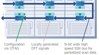
IEEE 1149.10, approved in May 2017, defines circuitry for testing ICs through a high-speed TAP with a packet encoder/decoder and distribution architecture through which instructions and test data are communicated. This particular approach has several advantages, including maintaining testability of the functional path, and being future-proof against future functional high speed protocols. It supports all major current and future HSIO PHYs and enables high, measurable test coverage of all functional logic. The standard by itself, however, is not sufficient.
In the session “The Advancement of 1149.10”, Siemens Digital Industries Software experts JF Cote and Geir Eide present “Bringing 1149.10 to life.”
This presentation describes a complete end-to-end solution built on 1149.10, developed through collaboration with semiconductor companies, ATE manufacturers, and test program generation software developers. The goal of this approach is to ensure compatibility with existing ATE hardware and a seamless flow for effective DFT implementation, EDA-to-ATE hand-off, and ATE bring-up. This includes a straight-forward augmentation of the IEEE 1450 STIL pattern format to handle parallel execution of patterns associated with multiple time-domains, automated bit and latency alignment, and other special aspects of signals and patterns essential to 1149.10. To maximize the throughput and provide flexibility in the on-chip handling of the test data, the 1149.10 hardware known as the Packet encoder/decoder distribution architecture (PEDDA) is integrated with an existing, highly effective, and scalable on-chip scan test data distribution network. This solution shows that HSIO-based scan test is not just possible, it is ready for the mainstream.
Accuracy and scalability of physically aware diagnosis for yield learning
Another Tessent presentation in the “Diagnosis and Yield Learning” session is from Tessent chief engineer Wu-Tung Cheng. He will talk about the progress made in scan test failure diagnosis and the challenges ahead.
Scan test failure diagnosis has been used successfully to identify defect location in semiconductor manufacture process. To reduce test cost, scan chain test compression has been used extensively and significantly reduce test data volume and test time. Although test compression impacts scan chain failing data information of each test pattern, reduced test data per test pattern allows more failing test patterns to be collected. Experiments have shown that enough varieties with more failing test patterns can achieve better diagnosis resolution even with higher test compression.
Significant research has been done on compression designs and data selection algorithms to achieve higher diagnosis resolution with higher test compression under the general hypothesis that all failing patterns are caused by the same defect. It shows that with bigger and more complex designs, better data management of various failing patterns is necessary to provide enough diagnosis accuracy and diagnosis resolution.
With modern day semiconductor manufacture process, systematic defects related to layout patterns and litho process are the major cause of yield issue. Although systematic defects are not at the same location, they are caused by the same root cause. Improvements in management of failing patterns leads to high accuracy in single root cause identification for yield improvement.