Thermal Influence on Maximum Current Carrying Capacity
Superconductors aside, anything that conducts electricity will dissipate heat. This so called Joule or Ohmic heating (VI or I2R) results in elevated temperatures of the conductor and its surroundings. The more current that flows, the more heat is dissipated, the hotter things will get. At some point a thermal limit is reached that imposes a maximum current carrying capacity constraint. For a fuse this limit, by design, is the melting point of the conductor. For a PCB trace it is often the glass transition temperature of the surrounding FR4 dielectric.
IPC-2221 and IPC-2152
IPC-2221 Section 6.2 provides information to help determining the required cross sectional area of a PCB trace, ensuring it is big enough so as not to resist the current flow unduly. The maximum allowable temperature rise, the difference between an ambient temperature and the maximum allowable temperature, is first determined. Then, using the relationships in ICP-2221, the required trace cross sectional area for a given current and temperature rise can be noted. There are various online calculators that incorporate these relationships. IPC-2152 superseded IPC-2221, with revised correlations, accommodation of the effects of a nearby plane, the thickness of the PCB and the dielectric thermal conductivity.
3D Electro-thermal Simulation
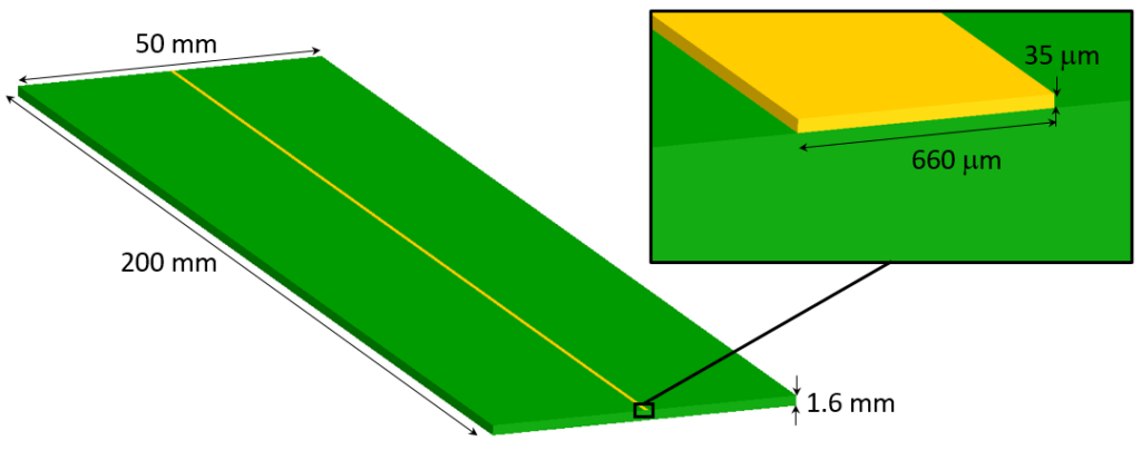
Electro-thermal simulation can be used to study the relationship between any routing structure and maximum current carrying capacity. It’s always good to start simple so, using Simcenter*, I created the following 3D model of a single Copper trace on the surface of an FR4 substrate:
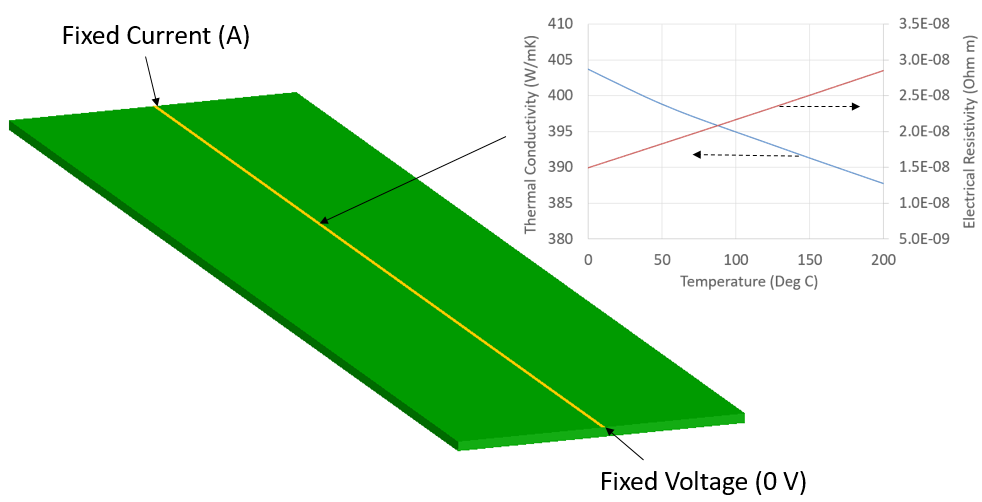
Electrical boundary conditions are applied on either end of the trace, fixed current at one end, a fixed voltage of 0 V at the other. From a thermal perspective a heat transfer coefficient of 10 W/m2K was applied to all faces on the top and bottom sides of the model with an external ambient temperature of 45 degC. The 4 other sides were set as symmetry:
Joule heating is a kind of double whammy. Joule heating losses increase the temperature that both decreases the thermal conductivity and increases the electrical resistivity. The latter leads to more heat being generated, the former leads to things getting hotter. If the heat isn’t removed efficiently enough, then you get thermal runaway and everything melts. An electro-thermal simulation predicts both the current and voltage fields, the heat flux and temperature fields and the power<->temperature coupling between them.
Single Trace Results
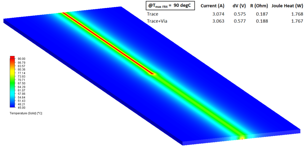
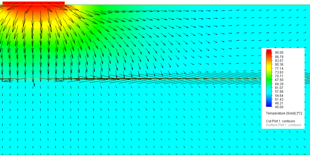
Both the DC electrical flow in the trace and the full 3D thermal distribution is solved. The steady state distribution of temperature, voltage drop, current density and Joule heating power dissipation distribution is predicted. A simple optimisation is performed so as to identify what current leads to a maximum limit temperature of 90 degC:
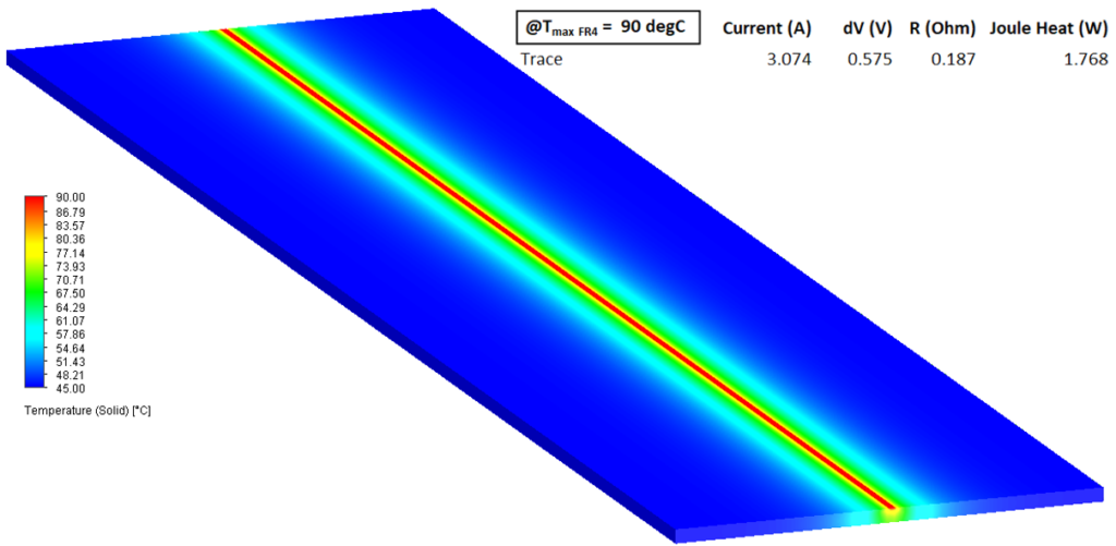
Remember that the only operational input to the model is the supply current, all other parameters are predicted. So in this case the maximum current carrying capacity is 3.071 Amps, resulting in a temperature rise of 45 degC.
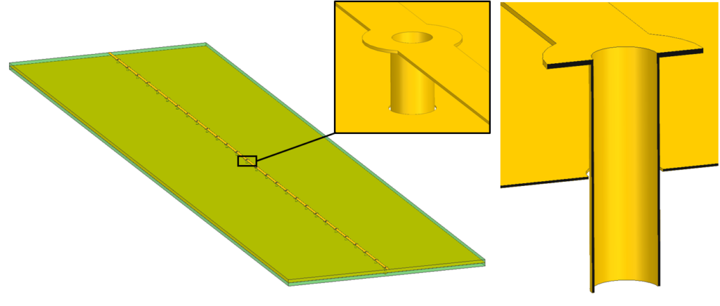
Adding a Via
A via is an electrical connection that links 2 traces that do not lie on the same PCB layer. A through hole via is a hole that is drilled all the way through the board and Copper deposited on its inner face. So, what happens to the maximum current carrying capacity when a via is included? Let’s model it:
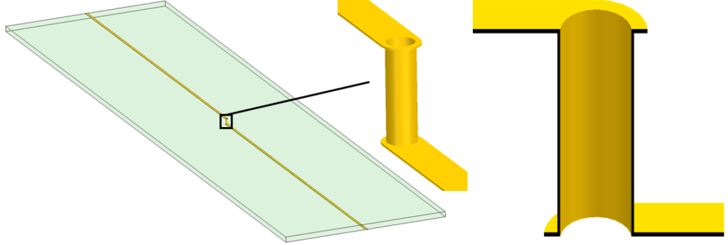
One half of the trace remains on the top of the FR4, the other half on the underside, the via connects them together.
From both an electrical and thermal perspective, it’s good practice to maintain the cross section area that the current (or heat) flows through. In this case, assuming a via plating thickness = 1/2 of the trace thickness and the Copper cross sectional area in the trace = the via plating annulus area, the via drill diameter is determined analytically.
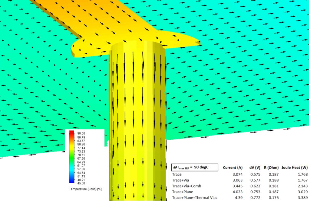
The maximum current carrying capacity hardly changes compared to the single one sided trace. A small portion of the trace goes through the thermally insulating FR4 so will get slightly hotter. But this is balanced by the fact that splitting the trace over 2 opposite surfaces increases the available cooling, slightly.
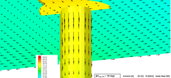
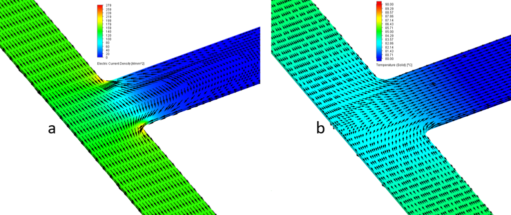
The simulation enables an insight into the electrical and thermal behaviour of the via:
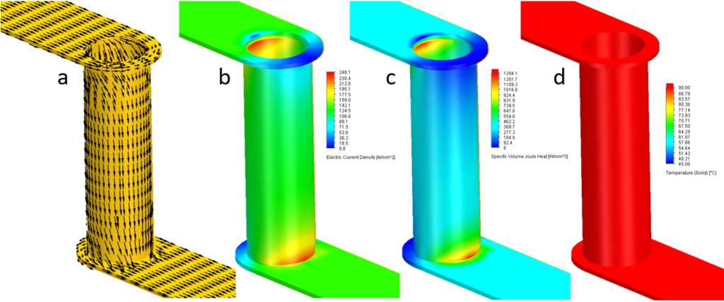
Most of the current enters the via one the side where the trace attaches, same for the current leaving the via on the bottom side. This does cause some current crowding which results in localized ‘hot spots’ from a Joule heating power dissipation perspective. However not ‘hot spots’ from the thermal perspective. Even though, locally, power density can be quite high, due to the high thermal conductivity of the trace the heat conducts readily from those areas resulting in a highly uniform temperature distribution.
Adding a Heatsink ‘Comb’
The term ‘heatsink’ is a bit of a misnomer. Heat isn’t magically sunk away, at least not under steady state DC type conditions. Instead a heatsink is better described as an ‘area extender’. It acts so as to spread the heat to a wider surface area so that it can be convected or conducted away more readily, thus reducing temperature rise.
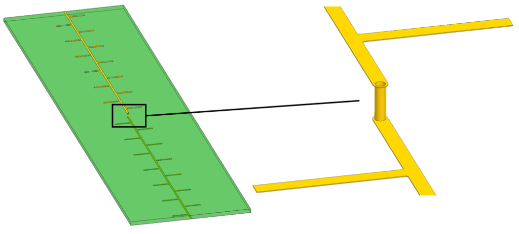
Tines are added, perpendicular to the trace, with the intention of reducing temperatures, rather increasing the maximum current carrying capacity:
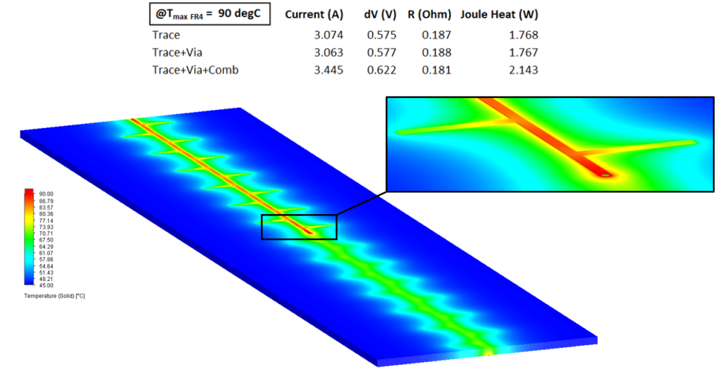
The maximum current carrying capacity increases by 12% due to the cooling effect of the comb heatsink tines. The electrical resistance decreases by 4% due to the fact that, even though the maximum temperature is still 90 degC, other areas of the trace are at much lower temperatures.
Wouldn’t the tines have more of an adverse effect on the electrical resistance?
The tines are stubs, cul-de-sacs from an electrical perspective. There is only a slight detour of the current into and out of where the tine meets the original trace. Thermally however they are ‘grounded’ and so heat rushes from the Joule heated trace, up the tines then out into the board and from the tine surface.
Caution – Heat Flows from Hot to Cold
If a trace is hotter than its surroundings, heat will flow from it. Any type of area extension will help that heat leave more effectively. If however the surrounding area of the board is hotter, for example a high power active is placed nearby, then the opposite will be true. The extended trace area will act so as to effectively collect/gather that heat and further increase the trace temperature.
Other Ways to Spread the Heat
It’s naïve to assume that there might be enough free unrouted space to consider using tines. It served only as a pedagogic example of the benefit of heat spreading. In the above models there were no internal PCB layers, just a single trace. An internal layer can itself help to spread the heat:
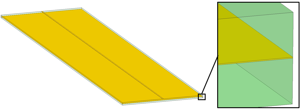
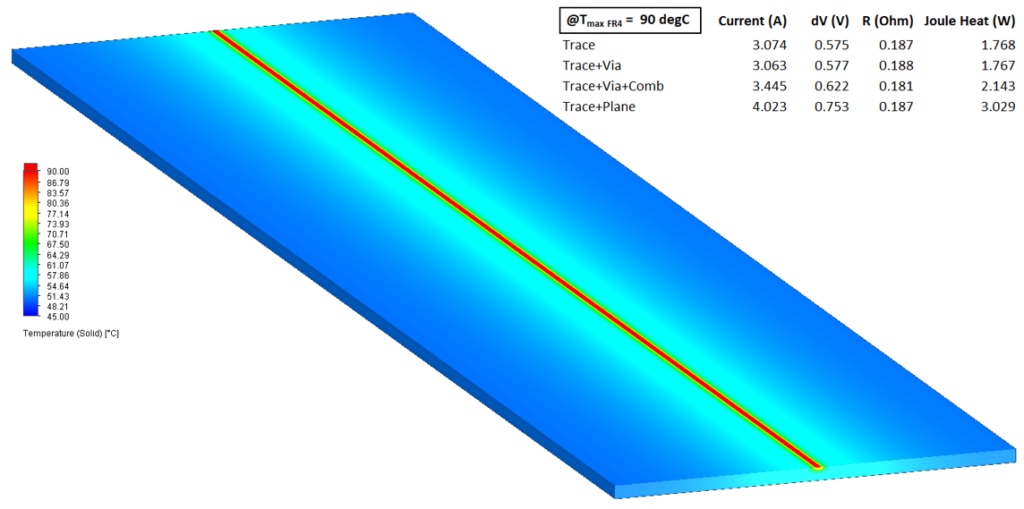
Even though there is no direct electrical connection between the trace and plane, there is a thermal connection. FR4 is ~1300 times worse at conducting heat than Copper, still it does conduct heat down to the plane where it then spreads laterally, then back out through the FR4 to the top and bottom PCB faces:
The end effect is to enable a 31% increase in current carrying capacity. So the plane is a great heat spreader, how could it be better utilised? Getting the heat from the trace down to the plane more effectively than having to pass through the FR4 would be good. This can be achieved with the use of thermal vias. Same as electrical vias but serving no other purpose than to get the heat (as close as possible) to internal planes whereupon it can spread out:
The trace cross sectional area is preserved as it goes round the top of the via and the plating thickness is again 1/2 of the trace thickness. There is no direct contact between the via and the plane, just as small as possible a thermally resistive gap of FR4.
The maximum current capacity is now increased 43% compared to just a single trace.
All the above studies considered DC conditions only. Under high frequency conditions it’s possible that other untoward SI effects might manifest due to the ‘stub’ type features modelled, that admittedly are beyond the scope of this blog.
Simcenter and Hyperlynx
There are various Siemens Digital Industry simulation softwares that can be used for these types of studies. From the Simcenter portfolio these include *Simcenter FLOEFD, Flotherm, Flotherm XT, STAR-CCM+ and 3D. Each has their own strengths, capabilities and target user personas.
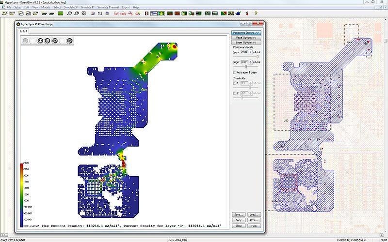
When it comes to dedicated PCB level simulation, be it SI, PI, DRC etc. the Hyperlynx portfolio is the tool of choice. Hyperlynx PI can be used to study voltage drop in PDNs, has the ability to perform electro-thermal co-simulations (either in its own environment of co-simming with Simcenter Flotherm XT or FLOEFD) and can export PDN powermaps for use in Simcenter Flotherm. Whereas the studies in this blog focused on single traces, Hyperlynx really comes in to its own studying fully routed designs, current crowding due to necking in PDNs, how that affects Joule heating and subsequent thermal knock-ons.
Check out this HyperLynx PI demo video for more details!