Advanced thermal design strategies for 3D IC systems

Not long ago, OpenAI CEO Sam Altman remarked that advanced AI video generation workloads were pushing GPUs toward their thermal limits. While dramatic, the statement reflects a very real engineering challenge in today’s AI and high-performance computing (HPC) systems:
As chips become smarter and more powerful, do they inevitably run hotter?
With 3D ICs becoming the foundation of next-generation AI accelerators, thermal management is no longer a secondary design consideration. In stacked die configurations, heat flow is constrained in three dimensions, actively limiting achievable frequency, expanding guardbands and introducing earlier-than-expected reliability risks.
This article examines advanced thermal design considerations specific to 3D IC packaging. It explores how thermal behavior in stacked architectures differs fundamentally from traditional 2D monolithic SoC designs, outlines key challenges unique to heterogeneous integration and presents practical strategies for building thermal confidence into modern 3D IC packaging workflows.
Why thermal management is more challenging in 3D IC packaging
The fundamental laws of heat transfer have not changed. What has changed are the boundary conditions. In 3D IC packaging, architectural and packaging decisions amplify thermal constraints that were manageable in planar designs.
Figure 1. Illustration of thermal distribution in a 3D IC package.
#1 Vertical stacking increases thermal resistance sensitivity
Stacking dies up increases localized volumetric power density while restricting natural heat dissipation paths. In most 3D IC systems, the primary heat sink remains on one side of the stack. Intermediate dies must dissipate heat through multiple material interfaces before reaching that boundary.
Each additional interface (bonding layers, micro-bumps, underfill and substrates) adds thermal resistance that compounds vertically. As a result, small changes in interface properties or stack order can produce disproportionately large temperature differences across the system.
Unlike traditional 2D monolithic SoCs, where lateral heat spreading dominates, stacked architectures introduce strong vertical conduction bottlenecks. Thinned dies reduce in-plane spreading capability, making junction temperature highly sensitive to vertical stack configuration. In high-power AI accelerators, modest packaging changes can shift hotspot locations or increase peak junction temperature by double-digit degrees Celsius.
#2 Thermal coupling becomes systemic
In 3D architectures, temperature change within one die can elevate temperatures in adjacent dies through shared vertical conduction paths, even when each die independently meets their thermal limits.
For instance, a high-bandwidth memory (HBM) stack can alter the thermal gradient of a neighboring compute tile. A logic die can pre-heat stacked memory layers beneath it. Such coupled effects often emerge late in the design cycle when packaging-level thermal modeling is either simplified or disconnected from early architectural planning.
Complexity is further intensified by structural and material factors intrinsic to advanced packaging, including:
- TSVs acting as unintended thermal bridges
- Micro-bump arrays modifying local thermal resistance distributions
- Thinned dies diminishing lateral heat-spreading capability
- Anisotropic and temperature-dependent material properties influencing conduction behavior
#3 Traditional thermal analysis flow is unscalable
In traditional 2D IC flows, thermal validation is often performed late in the design cycle and driven by domain specialists. In 3D ICs, that sequencing leads to late-stage surprises, including hotspot escalation, gradient-driven reliability risks, EMIR sensitivity shifts and thermo-mechanical stress interactions.
To ensure reliable AI system performance, thermal analysis must shift left — into early architectural planning and stack definition — where design flexibility still exists.
EDA vendors such as Siemens support this shift by integrating early-stage thermal feasibility analysis with progressive refinement toward signoff accuracy. Designers can begin with limited inputs and incrementally incorporate detailed power maps, layout data and material parameters as the design matures.
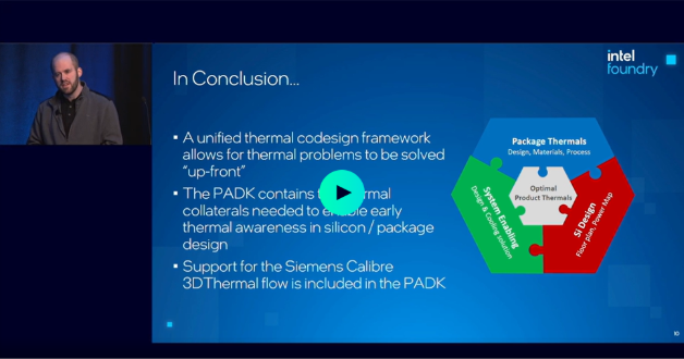
Figure 2. Intel Foundry presentation: 3D IC thermal workflow
Watch the Intel Foundry video to see how Siemens collaborates to streamline 3D IC thermal analysis. Discover how the integrated workflow enables electronics designers to run early-stage thermal simulations using Calibre 3DThermal from architectural planning through final signoff while accelerating model creation and refinement for thermal domain experts.
Four key thermal design considerations in 3D ICs
As integration density increases, several recurring thermal risk modes consistently surface in advanced 3D IC packaging flows.
#1 Address hotspot amplification
In vertically integrated stacks, high-activity functional blocks positioned away from primary heat removal paths (heat spreaders, lids, cold plates) are particularly vulnerable. Thinned silicon reduces lateral heat spreading capability, while stacked bonding layers and micro-bump interfaces introduce cumulative vertical thermal resistance. The result is amplified thermal sensitivity: localized junction temperatures can escalate rapidly under peak AI workloads.
Because thermal impedance is strongly influenced by stack order, interface material selection and bonding configuration, these decisions lock in thermal behavior early. Once defined, mitigation options narrow significantly. Late-stage thermal violations frequently force architectural compromises including frequency reduction, power throttling or guardband expansion directly impacting performance targets.
#2 Validate thermo-mechanical stress
Sustained temperature gradients across dissimilar materials introduce cyclic thermo-mechanical stresses due to mismatched coefficients of thermal expansion (CTE). In 3D stacks, these stresses concentrate in micro-bump arrays, hybrid bonding interfaces, TSV regions and underfill layers.
Even when average die temperatures remain within specification, spatial gradients and transient swing, especially under bursty AI workloads, can accelerate fatigue mechanisms, including interconnect cracking, delamination and interface degradation. Over time, these effects degrade long-term reliability and may erode yield, even when static thermal summaries appear acceptable.
#3 Verify thermal interactions at system levels
In traditional flows, thermal verification is often performed late and driven by simplified models or abstracted boundary assumptions. In dense 3D IC architectures, this approach underrepresents inter-die thermal coupling, interface resistance variability, material anisotropy, etc.
At advanced packaging densities, thermal verification must carry rigor comparable to timing closure or power integrity signoff. When thermal fidelity is insufficient, teams compensate through conservative guardbanding, over-designed cooling solutions or worst-case modeling assumptions. In the most severe cases, incomplete thermal modeling leads to post-silicon performance degradation where silicon meets power targets, but sustained workload operation reveals hidden thermal bottlenecks.
#4 Avoid overrelying on cooling to fix what the stack cannot dissipate
In many 3D IC programs, teams assume that increasing cooling capacity will resolve thermal challenges late in the design. However, materials and internal interfaces, such as thermal interface materials, underfill layers, interposers and substrates, often dominate the overall thermal resistance of the stack. When these internal heat paths are constrained, stronger external cooling may lower the average temperature but leaves localized hotspots only partially improved.
As a result, designs can continue to face thermal limits despite significant investment in cooling solutions. In practice, optimizing die placement, stack structure and interface properties early often delivers greater thermal benefit than downstream cooling enhancements. This is why packaging- and stack-level thermal evaluation should occur before finalizing the cooling strategy, ensuring internal thermal bottlenecks are addressed rather than masked.
Key thermal design strategies for 3D ICs
#1 Thermal-aware floorplanning
In 3D IC architectures, thermal analysis must resolve both vertical and lateral heat conduction paths, including die-to-die coupling, micro-bump and hybrid bonding interfaces, TSV thermal bridges and interposer / substrate conduction. As thermal behavior evolves with design decisions, simplified die-only models or abstract boundary assumptions cannot capture these effects with sufficient fidelity for architectural decisions.
Thermal-aware floorplanning is paramount. IC designers introduce rough predictive thermal inputs early, such as estimated power maps, simplified stack assumptions and first-order boundary conditions to anticipate where hotspots may develop and how heat will propagate across dies and through the package. These early models don’t need signoff-level accuracy. They need to be directionally correct so architects can move high-power blocks, separate competing heat sources or adjust die ordering while flexibility still exists.
To support this approach, the EDA flow must allow early power-to-thermal correlation, fast abstraction-level modeling and consistent handoff from architectural exploration to detailed multiphysics analysis. Thermal data need to stay synchronized as floorplans evolve. This increasingly requires an integrated flow that bridges chip, package and system domains.
EDA tools such as Calibre 3DThermal enable detailed die-level and stack-level thermal analysis within the design environment, while Simcenter Flotherm extends visibility into package and system-level cooling behavior. Electro-thermal and multi-physics approaches extend this capability further by connecting electrical activity, power delivery and mechanical stress to temperature behavior. Together, these capabilities support a closed-loop methodology: early predictive inputs guide floorplanning and progressively refined models validate multiphysics interactions through signoff.
Figure 3. Calibre 3DThermal embeds an optimized custom 3D solver of Simcenter Flotherm into the proven Calibre platform.
#2 System-Driven Thermal Co-Design
In 3D IC systems, thermal behavior must be treated as a system-level design variable, evaluated alongside electrical performance, power delivery integrity and mechanical reliability from the earliest architectural stages.
Rather than addressing heat after placement or packaging decisions are fixed, a system-driven co-design approach integrates predictive thermal modeling into floorplanning, stack definition and package exploration while meaningful flexibility remains. Relocating a high-activity block closer to a primary heat-removal path may increase routing complexity or congestion, yet substantially reduce peak junction temperature and long-term reliability risk. Adjusting die stacking order or interface conductivity can reduce thermal gradients and hotspot severity without altering total power.
Maintaining consistent thermal assumptions across abstraction levels improves correlation and enables predictable performance and reliability targets at signoff.
Figure 4. Siemens’ unified thermal design flow for 3D IC
Designing thermal confidence into 3D IC packaging with Siemens
As 3D ICs redefine what’s possible in AI and high-performance computing, heat becomes part of the innovation story.
Thermal confidence is built through integrated thermal co-design where architectural intent, packaging strategy and simulation fidelity evolve together.
Siemens is enabling this shift through fully integrated die-to-system workflows that integrate thermal analysis from early feasibility through final signoff. By linking architecture exploration, detailed implementation and multiphysics validation within a unified environment, teams can model thermal behavior progressively — refining accuracy as design data matures while preserving design flexibility.
Read the white paper to see how we can help building thermal confidence into your 3D IC designs from day one.
Frequently asked questions about advanced thermal considerations in 3D IC packaging
Why does packaging dominate thermal behavior in 3D ICs?
Interface resistance and vertical conduction limits introduced by bonding layers, underfill and substrates often outweigh die-level power effects. Packaging decisions define the primary heat removal paths.
What causes unexpected hotspots late in the design flow?
Hotspots typically result from die-to-die thermal coupling and interface assumptions that were oversimplified early. These interactions are only revealed when model fidelity increases.
How does advanced thermal modeling differ from basic analysis?
Advanced modeling explicitly captures die-to-die coupling, interface resistance and package-level effects rather than assuming uniform heat flow.
When should packaging-level thermal analysis begin?
During architecture and package exploration, before stack order, materials and boundaries become fixed.
Why doesn’t additional cooling always fix the problem?
If internal thermal resistance remains high, increasing cooling capacity lowers average temperature but does not eliminate localized hotspots. Packaging-level optimization is often required to change peak behavior. This is why stack-level thermal evaluation should occur before finalizing the cooling strategy.