How to Take Control and Reduce PCB Design Tweaking

In the realm of PCB fabrication, it is commonplace for manufacturers to “tweak” board designs provided by designers in order to improve yields. For those of you who may be unfamiliar with the phenomenon, here are some examples of design tweaking by the manufacturer:
- A simple tweak: Via pads are enlarged to meet annular ring requirements. In relatively simple boards, when there’s enough space on the layers to enlarge pads without getting too close to other copper features – it’s nice and easy. But in dense boards, there might not be enough space for this operation. In such a case, the pre-production engineer at the fab can do plenty of “creative” tweaking, from enlarging the pad non-uniformly to moving the other copper features further away, as shown in the drawing below.
- A less trivial tweak: When numerous vias pierce copper planes in dense areas, the vias are moved further apart from each other in order to avoid overheating during the drilling process.
- And lastly, a “real” tweak – staggering stacked vias: Stacked vias are expensive to produce. Fabs may attempt to unstack (or “stagger”) vias on inner cores. If it is possible to unstack all vias on the same core, then the production process becomes cheaper and more reliable.
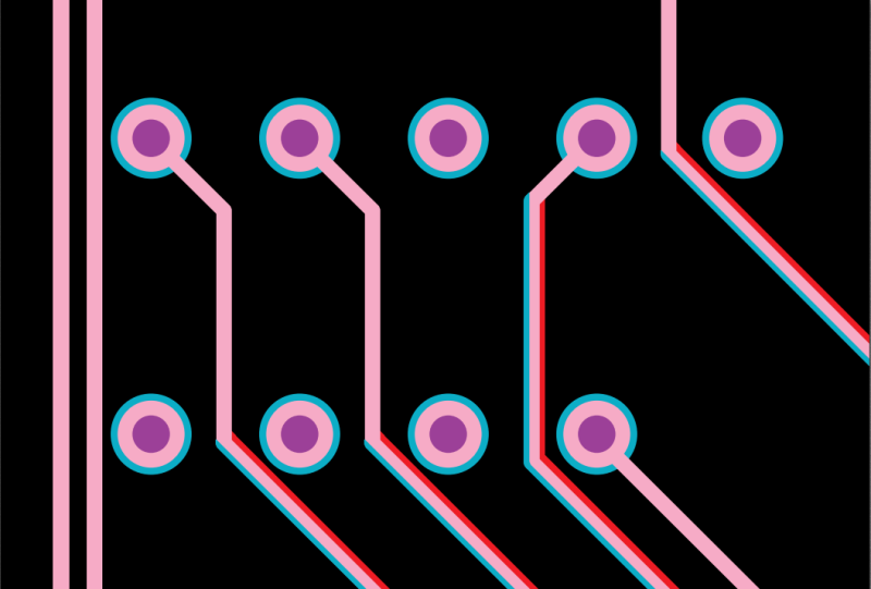
Example of moving traces away from a via pad, so that the pad can be enlarged in order to meet annular ring requirements.
• Red: trace path in original design
• Blue: trace path in tweaked design
• Pink: overlap of red and blue (area with no change in design)
• Dark pink: drills (for reference purposes only)
What are the risks involved in tweaking a board design?
In the vast majority of cases, the changes made by fabricators are minor and have no tangible effect on board functionality. Fabricators perceive design tweaks as an important part of their pre-production process, and invest lots of time and effort in making efficient, reliable and safe (from their point of view) design changes. They employ powerful CAM tools for PCB fabrication that assist in this. But since fabricators are typically unfamiliar with a board’s functionality, they are unable to judge whether or not a design tweak will cause new design or netlist violations (which is hard to check, since around half of all designs are provided without netlists) that will affect the board’s operation.
Here is an illustration of the risks, based on the simple tweak described in example 1 above.
Let’s say the preproduction engineer in a PCB fab decides to move a trace slightly away from a via pad so that the pad can be enlarged in order to meet annular ring requirements. In a majority of cases, this will not change the board’s functionality. But if this trace is an impedance control trace, then even a slight change in its position compared to adjacent layers can cause the entire board to exceed impedance tolerances – making the board nonfunctional (that is, scrap).
Or, the engineer might decide to “shave” an opposing copper plane to make room for the pad – without knowing that this plane serves as reference for impedance-controlled lines in an adjacent layer.
When is the impulse to tweak at its strongest?
The impulse to tweak a design grows along several axes:
- The larger the order (e.g. mass production vs. prototype), the greater the tendency to tweak the design, as yield factors become more critical.
- Fabs that focus aggressively on volume, lead-time and price reduction often initiate design tweaks without any formal engineering change request (ECR). More conservative fabs would not even move a silk screen without submitting a formal ECR to their customer.
- Large design houses have greater control over fabs than small ones do, so fabs tend to cut down on tweaks for designs that come from their larger customers.
- Lastly, inner layers are tweaked more frequently than outer layers – simply because tweaks on inner layers are not visible.
Tweaking and transparency
As a matter of course, it is expected that any design change would be submitted in advance to get the design owner’s approval. After all, this is a win-win situation for designers and fabs – since the fab can create the board with the same level of reliability at higher yields, it can pass some of the savings on to the designer. Yet, design tweaking is frequently performed during the fab process without the knowledge or consent of the designer.
In this rather delicate situation, fabricators that frequently request permission to change designs in a transparent manner may be perceived either as “highly reliable” or “annoying”. Clearly, the additional time and cost overhead that accompanies design changes and reviews may prove difficult for both sides to justify. New and innovative collaboration tools are needed to encourage such transparency.
Conclusion
In summary, here are some tips for designers that will help reduce the incidence of tweaking:
Minimize the need for design tweaks. If you’re aware of your fab’s yield considerations – take them into account in the design stage to avoid an additional round of design changes. This, however, requires a high level of trust between the fab and the designer. Fabs tend to minimize the amount of information they share on production capabilities, and are not always willing to share their yield considerations.
Here is where PCBflow can change the game. PCBflow is Siemens’ online Design-for-Manufacturing tool and collaboration space for PCB designers and manufacturers. Using PCBflow, fabricators build their yield considerations into their specific DFM profile that can then be used by designers to run their DFM analysis – without having to disclose their actual manufacturing constraints.
Provide the fab with additional information. Supply the fab with as much relevant data as is possible. Make sure that the netlist is included. For ODB++ users, this is simple. Designers use ODB++Design (OOD++D) to export all critical design data, converting it into a format that can be imported for use by any fabrication machine.
Sign up and try it now at https://www.pcbflow.com/ .


Comments