Sign In
Skip to content

Main Navigation

Blogs
  • Products
    • All Products
    • AMS Verification
    • Additive Manufacturing Software
    • Aprisa
    • Capital
    • Catchbook
    • Design with Calibre
    • EDA Consulting Services
    • Electronic Systems Design
    • Fibersim
    • HLS Design & Verification Blog
    • JT
    • Mendix
    • MindSphere
    • NX Design
    • NX Industrial Electrical Design
    • NX Manufacturing
    • Opcenter
    • PCBflow
    • PLM Components
    • Polarion
    • Questa
    • Semiconductor Packaging
    • Service Lifecycle Management
    • Simcenter
    • Solid Edge
    • Teamcenter
    • Teamcenter Manufacturing
    • Tecnomatix
    • Tessent Solutions
    • Valor
    • Valor DFM Solutions
  • Industries
    • Aerospace & Defense
    • Automotive & Transportation
    • Consumer Products & Retail
    • Electronics & Semiconductors
    • Energy & Utilities
    • Heavy Equipment
    • Industrial Machinery
    • Marine
    • Medical Devices & Pharmaceuticals
  • Podcasts
    • All Podcasts
    • 3D IC
    • AI Spectrum
    • Additive Manufacturing Podcast
    • Digital Powers Flexible: Consumer Products Podcast
    • Digital Transformation Podcast
    • Energy Transformation Podcast
    • Engineer Innovation Podcast
    • Innovation in the Classroom Podcast
    • Model Based Matters
    • Next Generation Design Podcast
    • Printed Circuit Podcast
    • Startups: Digitalization to Realization Podcast
    • Talking Aerospace Today Podcast
    • The Future Car Podcast
    • The Voice of Smart Digital Manufacturing Podcast
    • Where Today Meets Tomorrow Podcast
  • Thought Leadership
    • Thought Leadership Blog
    • Embedded Software
    • Expert Insights
    • Simulating the Real World
    • Verification Horizons
  • Corporate
    • Corporate Blog
    • AWS Partnership
    • Academic
    • Partners
    • Realize LIVE
    • Small & Medium Business
    • Xcelerator
    • Xcelerator Academy
  • Community
  1. Products
  2. Featured

ODB++

Copper layers on PCB

Old Habits Die Hard

February 1, 2021

In one of my previous blog posts, I asked the question: Why do designers keep sending Gerber files to their…

By Alex Belelovsky
3 MIN READ

Silkscreen – is it really that simple?

November 9, 2020

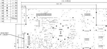
A silkscreen contains human- and machine-readable marks on the surface of a PCB that indicates PCB components’ positions and polarity,…

By Alex Belelovsky
3 MIN READ
Ensuring PCB design is ready for manufacturing

Skydiving without a parachute – how to enable exchange of manufacturing process requirements

October 12, 2020

On an August evening in the sky above a California desert, a skydiver leaped from the safety of an airplane…

By Max Clark
3 MIN READ
PCB design tweaks by manufacturers

How to Take Control and Reduce PCB Design Tweaking

September 30, 2020

In the realm of PCB fabrication, it is commonplace for manufacturers to “tweak” board designs provided by designers in order…

By Alex Belelovsky
4 MIN READ
Right-first-time PCB manufacturing

Right the first time

August 27, 2020

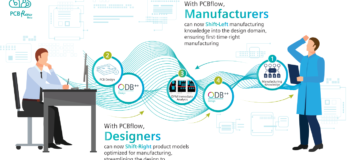
Shift left – Shift Right (1st part out of two) In 1887 the great city of Chicago in response to…

By Max Clark
2 MIN READ
Gerber fabrication drawing

Should You Really Trust Gerber?

July 23, 2020

The Gerber data transfer format has been serving the PCB manufacturing industry for decades, and the Extended Gerber standard (also…

By Alex Belelovsky
4 MIN READ