4 less obvious PCB DFM violations
The PCB design blogosphere is filled with articles listing rules of thumb to ensure your PCB layout is designed for manufacturing.
In this post, we dig a bit deeper to better understand what causes these manufacturability issues and identify some less obvious ones. With a deeper understanding of the cause, avoiding these issues becomes easier.
To better understand the issues that might arise, let’s first understand the PCB fabrication process.
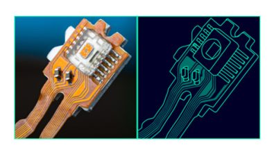
A simplified PCB fabrication process
- The starting point is a laminated board completely covered with copper. Contrary to popular belief, PCB designs are not “drawn” or applied to a board, but etched away.
- Layout is “printed” on the board using a protective layer that will prevent the copper from being removed in all required areas.
- Washing the inner layers of the board with acid chemicals that remove, or “etch” excess copper. This reveals the copper traces and pads.
- Stacking up PCB layers by laminating (heating and pressing) board materials at high temperatures.
- Drilling holes – through holes that connect layers (vias), and pin-holes for mounting components.
- Etching or removing excess copper from external layers. This is similar to step 3, but applied to different layers.
- Plating vias and pin holes to create connectivity between layers and components.
- Solder masking – applying a protective, non-conductive coating to protect the board and prevent unwanted circuits.
- Printing a final layer containing data and drawings
- An optional layer for design purposes
As complex as the process sounds, this is a simplified one. As you review the various steps, materials, and processes involved, it becomes clear how things can go wrong, especially with small, complex designs.
In addition, fabrication is only the first step in the board manufacturing process. After fabrication, components are connected to the board in assembly. Proper connectivity to these components is critical as well for proper board performance.
DFM is focused on ensuring that not only will board layouts be manufacturable, but that the fabrication and assembly process together generate a high yield rate, i.e. a high rate of properly functioning boards.
With that understanding, let’s have a look at some possible issues.
- Solder Mask clearance
In the solder masking process, certain areas where components will be added in assembly remain unmasked.
The main issue with solder masking is that it is not always accurate, meaning that solder mask, in reality, may slightly differ from the design. This partly depends on the method of solder masking that is being used (i.e., screenprint, curtain coat, HPLV air spray, or electrostatic spray). You can imagine that applying solder mask with an air spray cannot realistically deliver 100% accurate results. If in the design, the distance between areas requiring solder masking and areas that should not be masked is too small, then manufacturers risk covering a cleared area with solder mask by mistake – or vice versa.
Your solder mask clearance may be ok according to design rules. But in reality, there is a delicate balance between solder mask clearance and the distance between solder mask to non-exposed copper. The challenge here is to find the right compromise between the two and is a function of the accuracy of the manufacturing equipment used. More accurate fabrication equipment usually comes at a higher price, so the required clearance to be used in your layout, in a sense is a function of your business goals and target manufacturing cost.
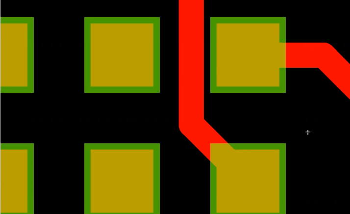
- The real issue with Annular Rings

An annular ring is an area of copper pad around a drilled and finished hole. Its width can affect your design and manufacturing considerations and determines how much the board can shift or a drill can move before electrical connectivity is impacted. It is a well-known fact that a wide ring ensures that the via remains within the pad and connectivity is maintained even if the drill moves off-center, while a thin ring increases the risk that the via will touch the edge of the pad. With the growing accuracy of drilling techniques, you may be tempted to think that annular ring concerns are a thing of the past.
However, there is an additional, just as important point related to annular rings which is plating. Through holes and vias are used to create connectivity between layers and between the board and its components. To provide this connectivity, holes need to be plated (step 7).
Proper plating requires sufficient annular ring width to attach properly and ensure connectivity. Too small rings can lead to inconsistent, or even totally missing connectivity. Furthermore, as holes are often used in inner layers, such issues are very difficult to correct, rendering an entire board useless if they happen.
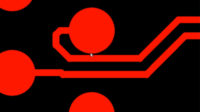
- Acid traps – more than just sharp corners
You may have noticed that acute angles have become common in modern PCBs. This is because many layout designers take pride in the unique shapes and designs they create. One of the reasons this is possible is that manufacturers have improved the etching process in recent years. From a manufacturability point of view, however, acute angles are not always a safe route to take due to their propensity to create acid traps.
An acid-trap is a layout that has the potential to trap chemical etchants used to strip excess copper from the PCB during the manufacturing process. The excess solution then corrodes other unintended areas the board, creating faulty connections or open circuits. The common layout rule of thumb used to avoid acid traps is to avoid sharp corners in the PCB layout. This is based on the assumption that if there are no sharp corners, then there is no place for the acid to accumulate. This approach however, is oversimplified. Sharp corners are in fact only a proxy for the real cause of acid traps – a layout that creates a small space where the acid can accumulate or become trapped.
In the image, you can see a potential acid trap that has no sharp corners.
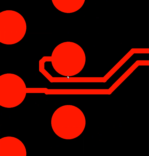
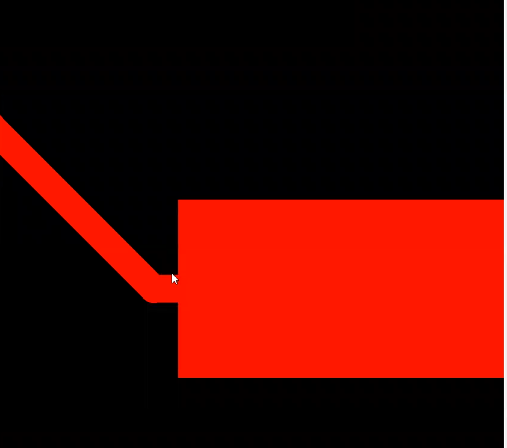
Consequently, a better rule of thumb for designers is to avoid small, nearly closed-off areas in PCB layouts. By leaving enough space, any traveling chemicals can move around adequately, rather than accidentally becoming trapped somewhere along the way.
- Power ground clearance in hole arrays
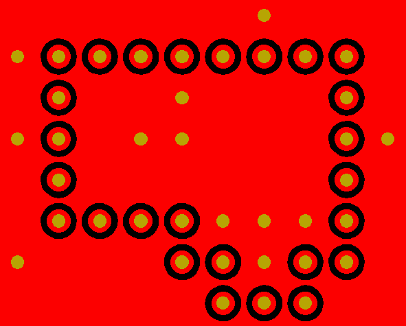
Many PCBs are multilayered, created as stacks of silicon wafers one on top of the other. These layers are connected through various routing options and together form a single PCB. Some PCBs are designed with a ground plane on one or more PCB layers. Adjacent to ground planes you can also find power planes, which carry the electric power flow of a PCB. Both the ground and power planes are crucial for the PCB’s electronic components to be connected with each other, and for electric power to flow safely between them, sustaining the system.
Power ground layers may include arrays or arrangements of holes, with clearance surrounding them. Imagine a very dense hole array where the clearance areas surrounding the holes are in close proximity leaving very thin copper connections to the inside of the array. We can imagine a situation where small variations in the location of the holes can cut off the current from the central area, consequently cutting off the current from the hole in the center of the array. the result is a disconnected power layer.
We refer to this situation as a copper bottleneck, whereby an unwanted change of the power ground layer’s original configuration leads to a “broken net”. As with many of the violations we discussed, a copper bottleneck may or may not occur during fabrication. but if it does, the board becomes useless.
Conclusion
In this post, we discussed the PCB fabrication process and how certain layout decisions may create faulty boards under certain circumstances. Armed with this understanding, you can make better design and layout decisions, based on your product and business goals. We have only scratched the surface, and the number of DFM considerations is too large to realistically cover them all. That is where automated DFM tools come into place. They check both common and not so common DFM rules for you so that you can reduce design spins and reach the market faster.
Start validating your PCB layout today
You can start validating your PCB layouts easily with PCBflow, a free, online Design for Manufacturing tool that leverages market-leading NPI software from Mentor and Valor. Simply upload your design to the secure cloud service that automatically checks your layout against nearly a thousand rules