NX | Tips and Tricks | PCB Exchange – Getting Started
In our latest NX™ software Tips and Tricks video, we dive into PCB Exchange and its use in analyzing IDX files in NX. In this video, we look at what settings are necessary, how to read new files, and how to view new layers and traces.
Check out the video below or scroll down to learn more about PCB Exchange.
What are IDX files?
Before we jump in, it’s important to understand what IDX files are. IDX, or Incremental Design Exchange files, are an XML-based file format that facilitates electrical and mechanical co-design and collaboration. These files contain board outlines, stackup structures, components, and board bend areas, among other items. Today, we’ll explore how to take an IDX file and use it to produce a CAD file for a circuit board.
PCB Exchange Preferences
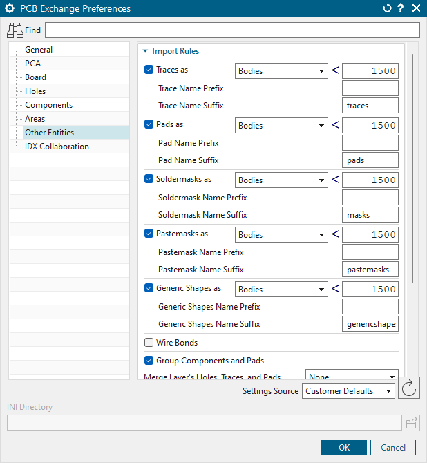
The first step in opening an IDX file in NX is to ensure that you have the proper settings selected. There are two sections in PCB Exchange Preferences that are crucial for this: Other Entities and IDX Collaboration.
Other Entities – Check the Traces, Pads, Soldermasks, Pastemasks and Generic shapes to ensure that each item imports as defined in the ECAD file. Additionally, set each item to load as bodies to create solid bodies with thickness for each item. This approach promotes the best visual experience.
IDX Collaboration – Select the proper file folder for your collaboration directory. This folder should be where you want PCB Exchange to store the IDX incremental files by default. NX stores this directory as an attribute on the current NX part, so the next time you open the part, NX recalls the directory.
Reading your IDX file
Now that we have selected the proper preferences, we can read our IDX file. To do this, we must select the Read PCB command, and then the file we wish to load. When we do this, we should also select “Only Use Existing Components” as well. After selecting OK, our file will load in.
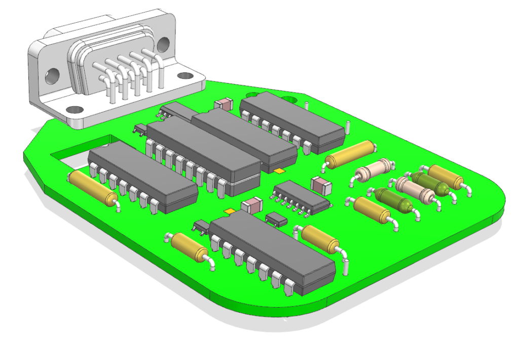
Once the file loads, we have a few ways to go about navigating our new assembly. One of the most valuable features of PCB Exchange is the PCB Navigator, found on the resource bar on the left-side of the screen. The PCB Navigator organizes all components and holes, making it easy to track part details such as package names and part numbers.
Additionally, another great tool for navigating our circuit is the Assembly Navigator, which organizes all imported parts. Selecting a part in either navigator highlights the respective part in the other navigator, as well as in the display window.
Adding design layers
Another important part of PCB design is including layers and traces in our model. To add these, we can use the Read Design Layers command. We are prompted to select a new IDX file, and this time, the ECAD layers, nets, and padstacks are included in our circuit.
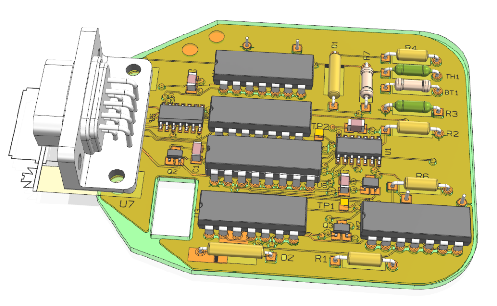
One easy trick to view the new PCB layers is to edit object display and change the translucency of the circuit board. This keeps the board visible as part of the assembly while providing insight into what it contains.
