Article Roundup: How Semiconductor Manufacturing Benefits from Smart Fabs, Parasitic extraction to guide capacitor usage in RF SoCs, Lower Resistance Protects Against Failure In IC Design, EDA in the cloud boosts DRC iterations for AMD, How to achieve fast, automated, sign-off verification of DFM hotspot fixes in P&R
- How Semiconductor Manufacturing Benefits from Smart Fabs
- Parasitic extraction to guide capacitor usage in RF SoCs
- Lower Resistance Protects Against Failure In IC Design
- EDA in the cloud boosts DRC iterations for AMD
- How to achieve fast, automated, sign-off verification of DFM hotspot fixes in P&R
How Semiconductor Manufacturing Benefits from Smart Fabs
Allaboutcircuits.com
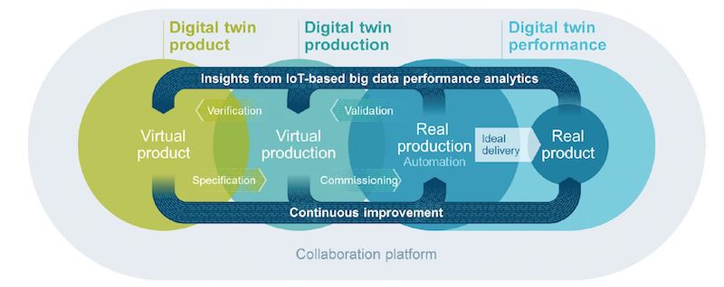 This article discusses the benefits of continually optimizing manufacturing for the semiconductor industry by introducing smart manufacturing solutions. The author talks about how the concept of a digital twin is heavily used in industries such as aerospace, defense, and automotive. Semiconductor fabs are ahead of the curve on implementing smart manufacturing, but the capabilities are myriad and quickly evolving. This article also throws light on where smart manufacturing is now, and more about closing the loop on design, build and test in IC design.
Parasitic extraction to guide capacitor usage in RF SoCs
TechDesignForum
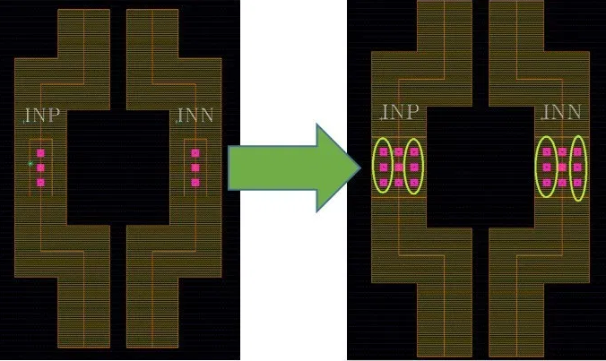
 Mentor’s xACT platform offers analog/RF designers the fast performance of a rule-based extraction engine, and the capacity and performance of a field solver, to efficiently extract all parasitic components in a timely manner, with the confidence that all parasitic effects are accurately characterized. This article throws light on parasitic extraction to guide capacitor usage in RF SoCs and more.
Lower Resistance Protects Against Failure In IC Design
SemiEngineering
 At advanced nodes, increasing resistance means IR drop and EM issues have become significant performance and reliability detractors. Adding vias to the layout is the most effective means of reducing the impact of these effects, but traditional custom scripts are difficult and time-consuming to create and manage, without the guarantee of correct by construction vias. This article talks about how PowerVia utility automated via insertion flow can increase design reliability and reduce IR drop. To evaluate the effectiveness of the new approach, Mentor collaborated with integrated circuit (IC) design companies to implement and evaluate the use of the PowerVia solution in production designs.
EDA in the cloud boosts DRC iterations for AMD
TechDesignForum
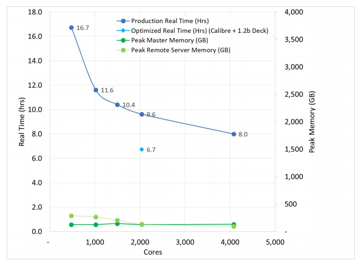 This article talks about the recent collaboration between AMD and Microsoft Azure, and how the chip company was able to increase its design-rule check iterations on a 7nm full reticle design from 1-1.5 times a day based on internal resources, to 3 times a day by transitioning to running DRC EDA in the cloud. Physical verification happens at the end of the design cycle, so when the design schedule invariably slips, enormous pressure is put on the verification team to complete more design iterations per day to achieve tapeout as quickly as possible. For any company, the impact of moving from one design turn per day to multiple turns per day will significantly compress their time to tapeout.
How to achieve fast, automated, sign-off verification of DFM hotspot fixes in P&R
TechDesignForum
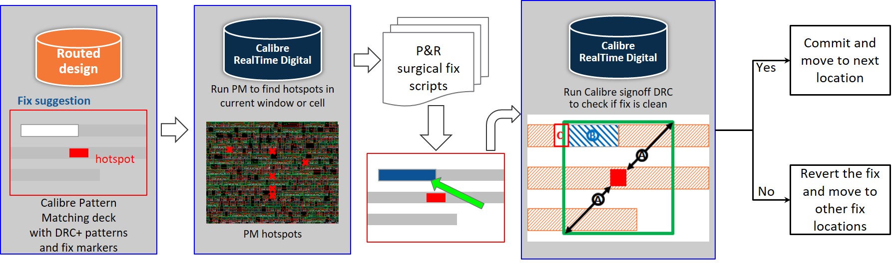 This article talks about automated hotspot detection, correction and verification in P&R. The articles highlights how the collaboration between Globalfoundries and Mentor’s pattern matching tool accelerates signoff DRC closure for their designs, potentially reducing tapeout. Locating and fixing DFM hotspots during design implementation is a challenging and time-consuming task, albeit one that has become essential given today’s complex manufacturing processes. Additionally, while facing market and resource constraints, design companies look to their EDA toolset for automated support for such processes.