Semiconductor design innovation: how EDA initiates the digitalization journey for a smarter, sustainable future.
Topic 3 in our Blog Series, “Sustainability in Semiconductors. Every Detail Matters.”
Hannover Messe 2024, the world’s leading industrial trade fair happening April 22-26 in Hannover, Germany, is just around the corner! Siemens is giving you a digital preview of the comprehensive range of solutions for semiconductor design and production on display at the event. Siemens’ theme this year: “Sustainable Digital Enterprise – Semiconductors” highlights how technology and industry ecosystem work together to achieve sustainable chip production.
Semiconductors, also known as integrated circuits or chips, are undoubtedly the foundation of digitalization. The performance and their capacity to process data for the vast number of electronic devices dictates what levels of digitalization can be achieved by companies and government entities around the world. For the past 50 years, the semiconductor industry has been able to double the number of transistors of ICs (cutting cost of each transistor in half) while simultaneously increasing the performance of integrated circuits (aka Moore’s Law). Keeping pace with Moore’s Law has over many generations been a herculean effort of continuous invention and collaboration between many industries, including capital equipment manufacturers, chemical companies, semiconductor companies or silicon foundries, mask makers, Electronic Design Automation (EDA) software companies and IC design teams within semiconductor and systems companies. Every two years has required refinements or even new manufacturing equipment, chemical mixtures, design techniques, EDA software and evermore qualified engineers.
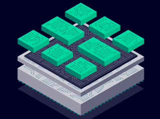
The challenges to continue this pace of IC innovation and thus digitalization are rapidly becoming exponentially more complex. Around 10 years ago, the physics underlying the ability to double the number of transistors on a single chip (monolithic die) began to falter. To get around this issue, the industry is looking upward. It is currently in the process of bringing to the mass market the era of 3D ICs, in which monolithic dies are stacked next to each other and, more challenging, on top of one another in the same footprint of a single monolithic die.
To bring 3D IC to light comes with all the challenges of monolithic die design but also new design and exponentially more manufacturing challenges that will require an even tighter and closer collaboration between all the industries that contribute to the creation of next-generation semiconductors. Simultaneously, all the companies within the semiconductor supply chain are being tasked with enacting new ways to reduce their impact on the environment.
Siemens is committed to helping the semiconductor supply chain continue or even exceed Moore’s Law while also reaching their sustainability goals. Perhaps an often-overlooked ally to help overcome this challenge is right in front of them – it’s the product they produce – ICs.
Semiconductor sustainability starts with design
In 2016, Siemens made a bold commitment to becoming a leader in helping customers accelerate their digital journey when it jumped into the EDA business by acquiring Mentor Graphics, the broadest line supplier and longest standing brand in the EDA business (producing the software electrical engineers use to design ICs, IC packages and printed circuit boards). Since that time, Siemens EDA has rapidly advanced toward the goal of becoming the broadest supplier of the best EDA technologies and the pioneer of leveraging AI in tools (software) to achieve better results faster.
With Siemens EDA technology added to Siemens Digital Industries Software business, Siemens became the first company to offer a full line of multi-physics solutions that bridge electronic engineering, software engineering, and mechanical engineering. This has given Siemens a distinct advantage in helping customers advance from monolithic to 3D IC design and has enabled companies to build a truly comprehensive digital twin of their components, their machines and someday even their factories.
With information about the end-goals of the system shifted left all the way to the IC design teams, ICs can be designed to have the correct mix of performance and power consumption and can be designed to more efficiently monitor or control the power consumption of the systems they run. They can be built to react more quickly to unsafe conditions. Meanwhile, Siemens is also a pioneer of Silicon embedded analytics, which will enable companies to monitor ICs running in the field over the IC’s lifetime. Silicon embedded analytics enables companies to identify failing systems, perform preventative maintenance, and gain information to design better next-generation ICs and even systems more proactively. Indeed, achieving manufacturing excellence with sustainable solutions starts with IC design.
Being that next-generation capital equipment and factory equipment are all controlled by ICs with the goal of manufacturing better next-generation ICs, it seems almost too obvious that the journey to reaching new levels of digitalization, and a smarter, sustainable future in the semiconductor industry can start with designing smarter ICs for their own equipment.
We invite you to visit our exciting Hannover Messe page to get your free ticket for Hannover Messe 2024! www.siemens.com/global/en/company/fairs-events/fairs/hannover-messe.html


Comments
Leave a Reply
You must be logged in to post a comment.
Fantastic insights on elevating energy business operations through capital asset lifecycle management paired with SAP. It’s crucial how the integration of such systems not only streamlines operations but significantly advances sustainability efforts in the energy sector. As organizations look to implement these solutions, the role of comprehensive digital strategy and precise marketing cannot be overstated. At https://my-pascoconnect.com we specialize in crafting digital marketing strategies that enhance online presence and drive engagement, crucial for businesses undergoing digital transformation. Partnering with a seasoned digital marketing firm can provide the visibility and traction needed to maximize the benefits of sophisticated asset management systems like SAP.