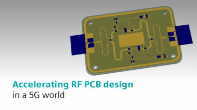
Accelerating RF PCB design in a 5G world

The demand for high-speed and efficient RF (Radio Frequency) PCB design has never been greater. With billions of IoT devices expected to come online in the coming years, the necessity for RF design capabilities supporting ultra-fast 5G speeds is becoming increasingly apparent.
The 5G revolution: why extreme speed support is crucial
Several factors are driving the demand for extreme 5G speed support in RF PCB design. These include:
- IoT: the Internet of Things is expanding at an unprecedented rate, with devices requiring higher frequencies and wider bandwidths.
- Connected vehicles: autonomous and connected vehicles rely on robust RF PCB designs to enable real-time communication.
- Smart homes & cities: these interconnected ecosystems demand reliable and fast RF connections for seamless operation.
- Connected health: telemedicine and remote health monitoring require high-speed and low-latency RF connections.
- Smart media, agriculture, industrial, and more: various industries are integrating smart technologies that rely on efficient RF PCB designs.
Compared to 4G networks, 5G promises:
- 10X less latency: reduced delay in data transmission.
- 50X more speed: significantly faster data rates.
- 1000X more capacity: greater bandwidth to handle more devices and data.
Key challenges in RF PCB design for 5G
Designing for 5G presents several challenges that need to be addressed:
- Scalable numerology: adapting to new frequency bands and modulation schemes.
- Higher frequency and wider bandwidths: meeting the demands of higher data rates.
- MIMO and beam steering: implementing multiple input, multiple output technologies and directional signal transmission.
- Over-the-Air (OTA) testing: ensuring reliable performance in real-world conditions.
- 5G New Radio (NR) coexistence: harmonizing 5G with other wireless communication systems.
RF-centric PCB design capabilities
To meet these challenges head-on, RF PCB design requires specific capabilities and features:
- Ground stitching vias: to shield RF circuits from interference.
- Restrictive clearance rules: tailored for RF to ensure signal integrity.
- Automated RF circuit arrangement: efficient grouping and arrangement of RF components.
- Meanders and via-stitching: for creating co-planar waveguides and maintaining signal integrity.
- Flood regions with vias: according to specific design rules.
- Import of complex RF shapes: for intricate designs and layouts.
- Chamfered corners: to reduce signal reflections and improve performance.
First-time right: the cost of design respins
The average cost of a design respin is a staggering $28,000. With such high stakes, it’s crucial to get the design right the first time. PCB design tools that support RF-centric capabilities offer a competitive advantage, enabling companies to stay ahead in the fast-paced 5G market.
Leading the way with analog/digital/RF co-design
RF designs have evolved over time from being standalone boards to being part of PCBs. They contain mixed technology, have multiple layers and are multi-functional systems. They contain not only RF but analog and digital components, interconnects, multiple layers of power and can have sensitivity to cross technology electrical interference.
To meet today’s RF PCB design challenges, solutions must manage this layered complexity by seamlessly integrating with RF design tools. They should also have built in intelligence to recognize RF structures to enable RF specific automation so designers can do their jobs faster.
Xpedition allows users to create RF schematic and physical structures, then place and modify them in the context of the PCB RF component. Information can be seamlessly imported using the dynamic integration between Xpedition and 3rd party RF tools like ADS and HFSS. When information is passed into the PCB domain from an RF design tool, Xpedition has built in intelligence that identifies parametric RF elements. This includes information like ground plane cutouts so when a circuit is edited or resized the cutouts adapt automatically.
Verification is critical in reducing design risk on PCB designs containing RF. Once a PCB design is created, it can be brought back into the RF design tool for optimization and verification against industry safety radiation standards. This bidirectional integration enables the quick and efficient exchange of data between the different design domains and eliminates the need for manually reentering RF design information in either domain.
The power of Xpedition can be used to enhance the mixed technology RF design flow further by enabling parallel design on a board which is useful for geographically dispersed teams. Managed block reuse can also be utilized to save time, manage obsolescence, and quickly add proven circuits to a design.
Xpedition maintains the digital thread throughout development of a mixed technology RF design by seamlessly integrating with RF design tools and intelligently managing RF design elements within the context of the PCB. You can see all of these capabilities in our demo video.
Advanced RF PCB design capabilities are essential to success
In conclusion, as 5G networks continue to expand and IoT devices proliferate, investing in advanced RF PCB design capabilities is not just beneficial—it’s essential for success in the 5G world. Embrace the challenges, leverage the right tools, and stay ahead of the curve with Siemens Digital Industries Software.
To learn more about RF PCB design with Xpedtion, tune into our LinkedIn Live session on May 30: Optimizing connectivity between Xpedition and HFSS for RF systems design


