Understanding the impact of hatched ground planes on PCB impedance
Controlling the energy within a printed circuit board is key to achieving success. At times, how we control and contain this energy is no easy task. Utilization of ground planes is how this can be successfully achieved.
Ground, typically referred to as a reference, plays a crucial role in signal integrity, electromagnetic interference, and electromagnetic performance. While solid ground planes are commonly used and are an industry best practice, especially when it comes to strip line and micro-strip routing techniques, hatched (or crosshatched) ground planes can be employed and present an interesting alternative with specific implications for impedance control.
Why would someone utilize a crosshatched ground plane over a solid ground plane? Personally, I am a “solid ground plane” kinda guy, and after speaking with many in my professional network, both PCB engineers and PCB fabricators, the common theme that continues to resonate to the top is that the industry best practice for PCB design is to implement solid ground planes, especially when impedance requirements need to be employed. One thing is for sure, no matter the spectrum you’re designing your PCB in: digital, analog, mixed signal, RF, or microwave, the performance of your PCB is one of the three perspectives that must be addressed, along with solvability and manufacturing.
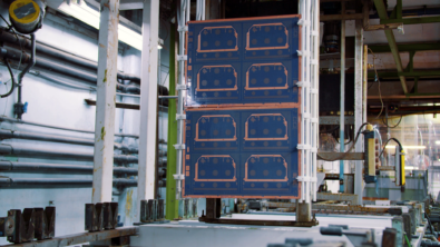
Typically, crosshatched ground planes are found in flex and rigid-flex PCB designs, more specifically in the flex portion of the design, for easier static or dynamic bending in a particular section of the design. Yet, there are those engineers who choose to employ the crosshatch approach into their ground plans instead of a solid ground plane.
Look, I know some experts, especially RF folks, get nervous when they see crosshatched ground planes being used for high-frequency signals. I’ve been there myself during design reviews. And yes, they’ve got a valid point about those longer return paths not being ideal. But here’s the real deal: when you’re working with flex and flex-rigid PCBs, crosshatched planes are actually a pretty clever solution, especially with today’s advanced materials and processes. From my experience in industry discussions and hands-on work, I’ve seen how they help maintain controlled impedance while keeping traces at manufacturable sizes, plus you get that crucial flexibility your board needs. The key is knowing how to properly implement these crosshatch ground planes when you need to maintain specific impedance requirements across the flex section. Sure, it might not be theoretically perfect from an RF purist’s perspective, but real-world applications have consistently shown that the practical benefits outweigh those theoretical drawbacks. It’s all about finding that sweet spot between perfect RF performance and what actually works in manufacturing. At the end of the day, it’s a solution that gets the job done, and gets it done well. So, let’s dive into how these patterns affect your circuit’s performance.
What Is a hatched ground plane?
A hatched ground plane (refer to Figure 1) consists of a mesh-like pattern of copper traces rather than a solid copper pour. This pattern typically forms a grid with open areas between the copper traces. The relationship between the copper and void areas can be expressed through the following impedance equation.


Key effects of hatched ground planes
Increased Impedance:
The primary effect of using a hatched ground plane is an increase in the characteristic impedance compared to a solid ground plane. This occurs because:
- The effective dielectric constant decreases
- The capacitive coupling between the signal trace and ground is reduced
- Return current paths become less direct
Return Path Considerations:
Hatched grounds force return currents to follow a more meandering path, which can be modeled as an increased inductance. This effect becomes more pronounced as the hatch spacing increases.
EMI Implications:
The gaps in hatched planes can lead to:
- Increased electromagnetic radiation
- Reduced shielding effectiveness
- Potential EMI compliance challenges
Best practices for using hatched ground planes
For optimal performance, maintain a hatch density of at least 70-80% copper coverage. The relationship between coverage and impedance can be approximated as:


Important note: PCB designers should use tools and simulations to determine optimal crosshatch patterns and opening sizes based on the specific application, signal characteristics, and impedance requirements.
- Pattern Orientation
- Align hatch patterns with signal traces where possible to minimize return path disruption.
- Critical Routes
- Avoid using hatched grounds under high-speed signals or sensitive analog traces where impedance control is crucial.
Advantages of hatched ground planes
- Better thermal stress distribution
- Improved PCB flexibility
- Reduced copper usage
- Enhanced adhesion in multilayer boards
Disadvantages of hatched ground planes
- Higher impedance variation
- Increased EMI susceptibility
- More complex impedance calculations
- Potentially reduced signal integrity
Conclusion
While hatched ground planes offer certain mechanical and manufacturing benefits, they significantly impact impedance characteristics and should be used with careful consideration. Simulation and analysis are a must and are key to achieving success. For critical high-speed designs, solid ground planes remain the preferred choice and industry best practice. However, understanding these effects allows designers to make informed decisions when hatched grounds are necessary or advantageous for specific applications.
In the end, and no matter what type of design your creating, remember to always collaborate with your PCB fabricator and validate your design through simulation, analysis, and testing, as the actual impedance effects can vary based on specific implementation details and manufacturing processes.