Cutting your losses – loss planning and you
When I started writing columns and blogs a few years ago, I wondered how much I’d have to say. An experienced media guy told me to watch my inbox for topics and questions that may be of general interest. That turned out to be excellent advice and here’s one such example.
“What is the best laminate for a loss budget of x dB for y inches? I was thinking in terms of Panasonic Megaton (sic) 6 or something like it.”
Megtron 6 is an excellent material, but it’s not cheap and it’s not the only horse in the race. In my response and in this article, I decided to focus on a loss planning and material-planning methodology rather than making a firm material recommendation.
Why we care about loss planning
Everything that improves material performance—and in this case, reductions in loss—comes at a price. Loss versus cost is a classic optimization problem: ideally, hardware designers want to pay just enough to meet loss requirements, but not more than they need to.
In the past, speeds were slow, layer counts are low, dielectric constants (aka: Dk or Er) and Loss Tangents (aka: Dissipation factor, Df) were high, design margins were wide, copper roughness didn’t matter, and glass-weave styles didn’t matter. We called dielectrics “FR-4” and their properties didn’t matter much.
As speeds increased in the 1990s and beyond, PCB fabricators acquired software tools for designing stackups and dialing in target impedances. In the process, they would acquire PCB laminate libraries, providing proposed stackups to their OEM customers fairly late in the design process, including material thicknesses, copper thickness, dielectric constant, and trace widths — all weeks or months after initial signal-integrity simulation and analysis should have taken place.
As speeds continued increased further in the 2000s, design margins continued to tighten and OEM engineers began tracking signals in millivolts (mV) and picoseconds (ps). FIGURE 1 shows these trends starting in 2000. Note the PCI Express trajectory in particular. Critical factors for signal integrity now include not only impedance, but loss, copper roughness, and glass-weave skew. Indeed, everything that happens in the process of physically building a PCB affects signal quality in a negative way and the details need to be accounted for across not just one PCB stackup, but across stackups from every PCB fabricator involved with a design.

FIGURE 1. Interconnect-speed increases in gigabits per second (Gbps) from 2025.
10 dB interconnect loss at 10 GHz
Using round numbers for an example, let’s say we’re targeting 10 dB total interconnect loss at 10 GHz for a 10-inch stripline run length using half-ounce copper. We’ll ignore vias for this example and just focus on the laminate. Experience says that this may require a material that’s indeed in the Meg6 range or better, but we don’t want to spend any more money than we have to, so we’ll start with a loss tangent (dissipation factor, Df) of 0.010 (more like Meg4) and see where we’re at for a starting point.
FIGURE 2 shows the result, but some explanation is in order. The blue line represents total loss, which is the sum of all other sources of loss. The orange line is conductor (copper) loss, which is the sum of skin-effect loss (red) and copper roughness (magenta). The graph shows loss in dB per inch, resulting in a total interconnect loss of 14.63 dB, a good bit above our target of 10 dB.
The next place I look is the Insertion Loss box, which is expanded in FIGURE 3. The two biggest contributors to loss here are copper roughness at 0.55 dB/in., the dielectric loss at 0.48 dB/in. and skin effect loss at 0.42 dB/in. I know that we can cut dielectric loss in half by cutting the Df value in half, so let’s give that a try. Changing Df to 0.005 results in a dielectric loss of 0.24 dB/in., as expected since it’s a linear relationship, and a total loss of 12.2 dB—a significant improvement! FIGURE 3 also shows that loss from copper roughness at 0.11 dB/in is very close to our new dielectric-loss contribution.
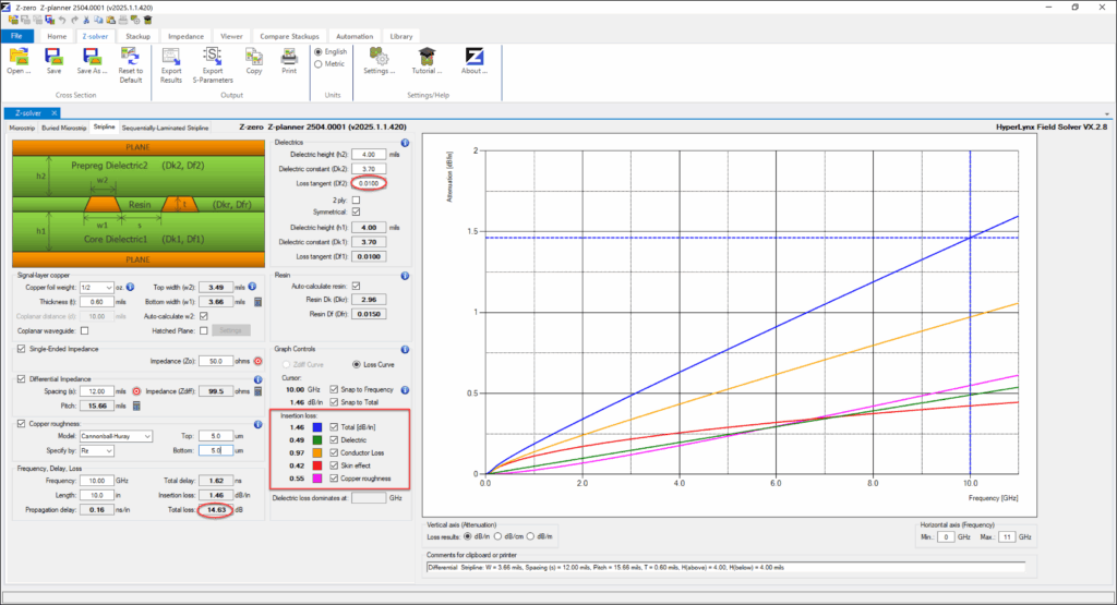
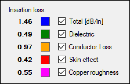
FIGURE 2 shows that the core-side roughness for this hypothetical laminate has an Rz roughness of 5.0 microns (um). This corresponds to what many call RTF or reverse-treated foil. I happen to know that materials in the 0.005 Df range generally offer smoother copper either by default or as a loss-reduction option. Let’s see what would happen with HVLP2 or “hyper very-low profile, 2 um” copper. FIGURE 4 shows this change, along with the resulting total interconnect loss, which is now 8.16 dB—meeting our total loss target.
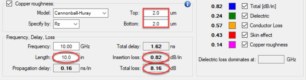
It’s interesting to note that the total insertion loss is now 0.82 dB/in. and that our total loss has over 1.8 dB of margin relative to our target of 10 dB. That means that we should be able to route this particular interconnect at 12 inches instead of our original 10 inches, or perhaps we could consider staying with 10 inches, and experimenting with a lower cost/rougher copper, and/or a lower cost material with a slightly higher Df and stay with 10 inches.
We do have some margin to play with, so if cost is a concern and we have the lead time, those are reasonable things to consider. It’s great having a “sandbox” to figure these things out. In fact, when we originally created this software utility, as part of Z-planner Enterprise, I called it “Field Solver Sandbox” (a bit long, so I changed it to “Z-solver”).
Further experimentation aside, we now have a Df target for a laminate system, a copper-roughness selection, and a routing rule. That’s a lot of progress early in the PCB design process. We can now begin looking for a material that aligns with these parameters.
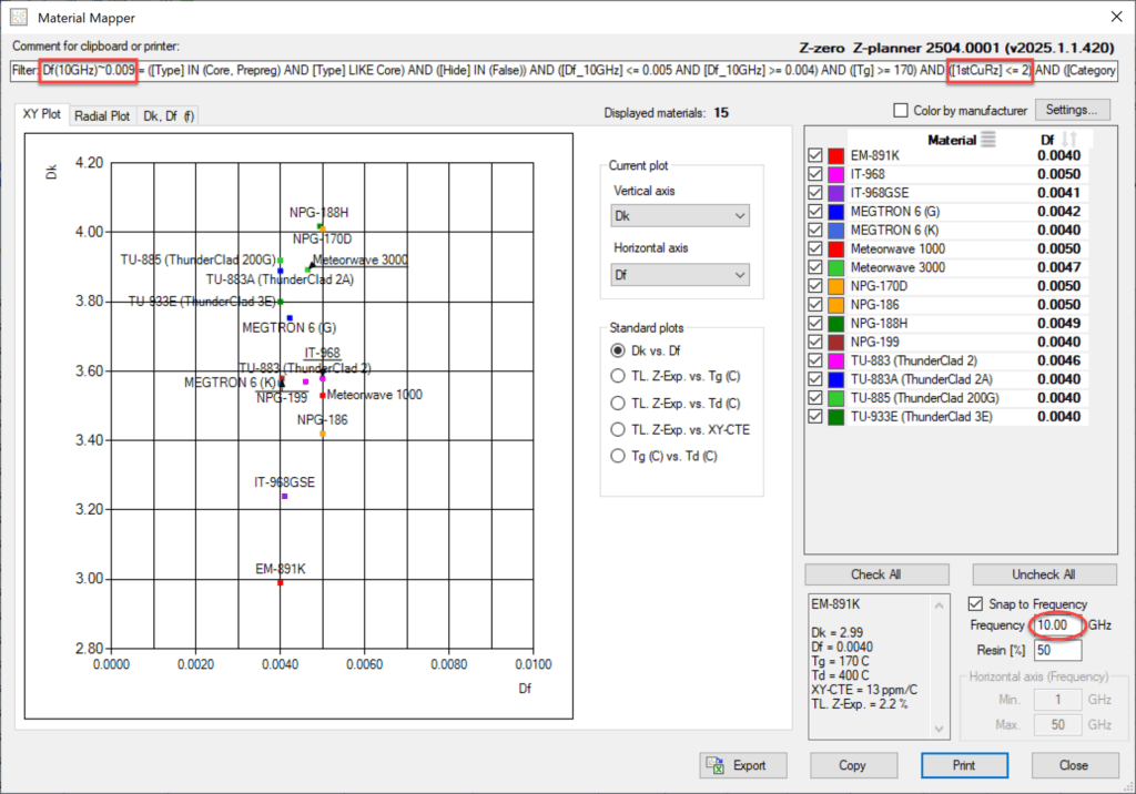
Two good places to initiate that search would be with your PCB fabricator(s) or from laminate-vendor data. Several materials that may be worth looking into are shown in FIGURE 5, based on their vendor-published Df numbers at 10 GHz and their published core-side copper roughnesses.
To come up with this list, I filtered Z-planner’s library of more than 290 laminate systems for materials with Df(10GHz) ≤ 0.009 and core-side roughness (Rz) ≤ 2 um. I also filtered for glass-transition temperatures (Tg) ≥ 170°C, which would be common for 14+ layer designs. The results were displayed using Z-planner’s “Material Mapper” utility, which is pretty helpful for visualizing multiple materials at the same time.
One thing that we learn from this is that laminates with roughnesses in the 2.0 um range (e.g., HVLP) tend to have Df(10GHz) values less than or equal to 0.005. If you know the laminate space well, that’s not much of a surprise, but it’s potentially instructive to know that loss tangents and roughness tend to be correlated in terms of material offerings from laminate vendors.
Wrapping up
If you can make material decisions early in the design process like this, you’ll be able to avoid prototype surprises down the road or paying more than you need to for laminate systems that are overkill for a design.
Making these choices early also allows you to avoid initial laminate lead times that can delay prototypes or early production. Because of prepreg shelf lives, fabricators only carry the laminates that they know they can use within six months or less, so a just-in-time approach is usually followed.
As in many other aspects of life, planning ahead gives you more options and fewer surprises. You can feed that expensive signal-integrity solution Dk and Df data from the actual laminate system that you’re planning to use. Moreover, it may allow you to hold to NPI (new product introduction) schedules more consistently, while at the same time relieving some of the pressure you’ve been putting on PCB suppliers to make up for poor planning … Everyone wins!