Etch effects exposed: discover where your copper really goes

Until recently, I thought that people who believed in rectangular traces were about as common as people that believe in square waves and a flat earth. Recently, though, I was asked about it and came to realize that it’s not as clear as I initially thought it was—not only for newbies, but in general. Over the last 25 years, I’ve acquired a good number of books on PCB design and signal integrity and you wouldn’t know from reading most of the industry literature that traces were anything but rectangular and that etching remained somewhat mysterious. Interesting, right?
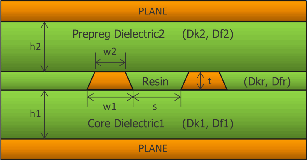
The stripline cross section in FIGURE 1 is from the Z-planner Enterprise software. Among other things, it shows that the base of a trace, facing the core dielectric, is wider than the side of the trace that faces the prepreg. As such, the trace trapezoids face both up and down in a multilayer stackup. There’s no relationship to the layer number or whether the trace is on the top or bottom half of the board. For this reason, I and others—but not everyone—avoid using terms like “top” or “bottom” as it regards trapezoidal traces.
In the dimensions shown in FIGURE 1, the w1 value at the base of the trapezoid is the value that hardware teams and fabricators exchange when talking about trace widths and spacing (s), but it’s important to know that actual, fabricated boards won’t have quite that much copper. As traces are etched from top to bottom, the etching chemical (“etchant”) remains in contact with the prepreg side of the trace longer than the core side. This makes the prepreg side of the trace narrower than the core side and gives the trace a trapezoidal cross section. In this blog we’ll discuss the reasons for this fabrication phenomenon and the implications for impedance.
Inner-Layer Etching
Etching inner layers involves cleaning the copper on both sides of the piece of laminate, applying a photoresist, exposing the photoresist to create the inner layer pattern, developing the resist, etching away the unwanted copper, and removing the etch resist. This process is automated in most shops and the chemistry is automatically monitored. As a result, the accuracy and repeatability is quite good. It is possible to etch inner layer traces using this process to an accuracy of ±0.5 mils. This accuracy control helps keep impedance within the tolerances required for transmission lines.
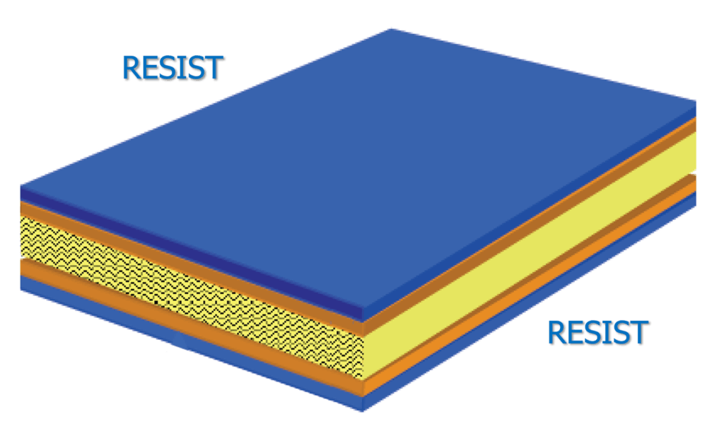
After cores are cleaned, FIGURE 2 shows a blue light-sensitive film or photo-imageable “resist” that is applied by heat and pressure to the metal surfaces of the core. The film is sensitive to ultraviolet light. If you ever tour a fab shop, the room where photo-resist is handled uses “yellow light” to prevent inadvertent exposure of the resist. The filters remove the wavelength of light that would affect the resist coating.
The GERBER or ODB++ data for the part is used to plot film that depicts the traces and pads of the board design. The photo tools or artwork include the copper features. This film is used to place an image on the resist.
Inner-layer film is a “negative” image of the copper features, meaning that the copper patterns left behind after processing the core correspond to the transparent areas on the film. Core panels are exposed to high-intensity ultraviolet light that serves to harden or “polymerize” the film resist, creating an image of the circuit pattern—very similar to a slide-negative and a photograph.
The exposed core is then processed through a chemical “developer” that removes the resist from areas that were not hardened by the UV light. Next, the copper is chemically etched from the core in all areas not covered by the remaining blue dry-film resist. After etching, the developed dry-film resist is chemically removed from the panel, leaving just the copper features exposed on the panel. It’s even a bit more nuanced than we’ve alluded to so far.
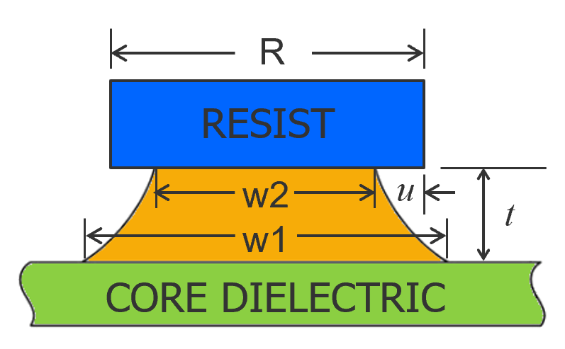
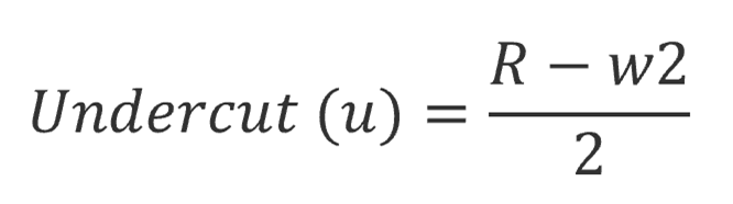
As FIGURE 3 shows, the actual sides of a trace will be curved and there is an etching “undercut” below the blue resist. Remember that w1 is the dimension that hardware teams and fabricators use to describe trace widths. R is the width of the resist that the fabricator uses. And the ledge under the resist is the undercut, u. Ideally, R, w2, and w1 would be equal. The closer that a fabricator can get to this, the better, and good fabricators work hard to achieve this.
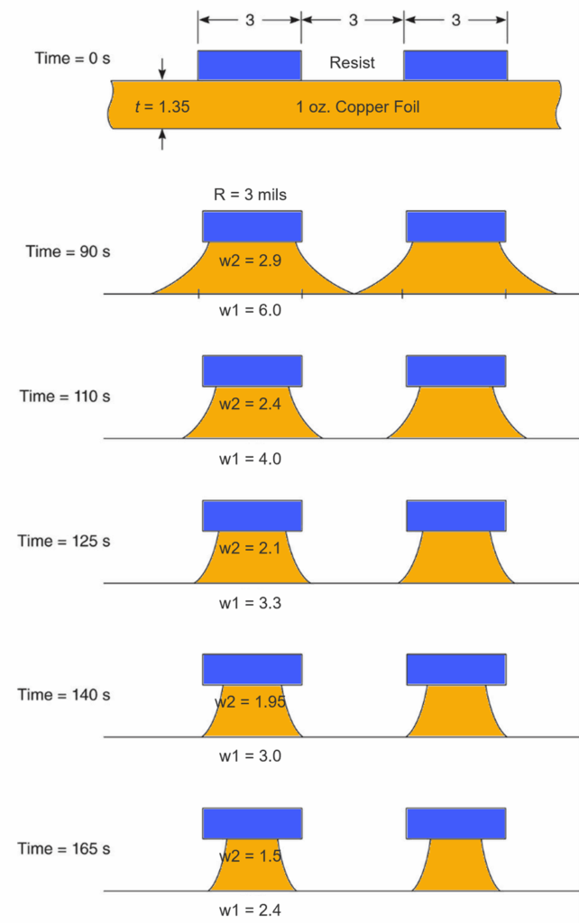
The gap between resist areas is removed evenly at first and then in a progressively cup-shaped fashion until the center area between traces is broken through to the exposed core dielectric, which opens progressively as the etchant goes to work in and under the resist as the side wall is gradually removed through increased exposure. The amount of time that the copper is exposed to the etchant determines the final shape of the copper features, as illustrated in FIGURE 4.
When the resist width (R) is equal to the base of the trapezoid (w1), this would be ideal etching. In FIGURE 4, this corresponds to the 140 second etching scenario. Note too that if R is less than w1, as in the cases up to 125 seconds, the copper features or traces are underetched. In the case where the copper is exposed to the etchant for 165 seconds, the copper is overetched. The times here are for this specific example, where cupric chloride was used as an etchant, targeting 3.0-mil line and space patterns, using 1.0-mil resist on 1-oz (1.35-mil) copper foil.
Etch Factor
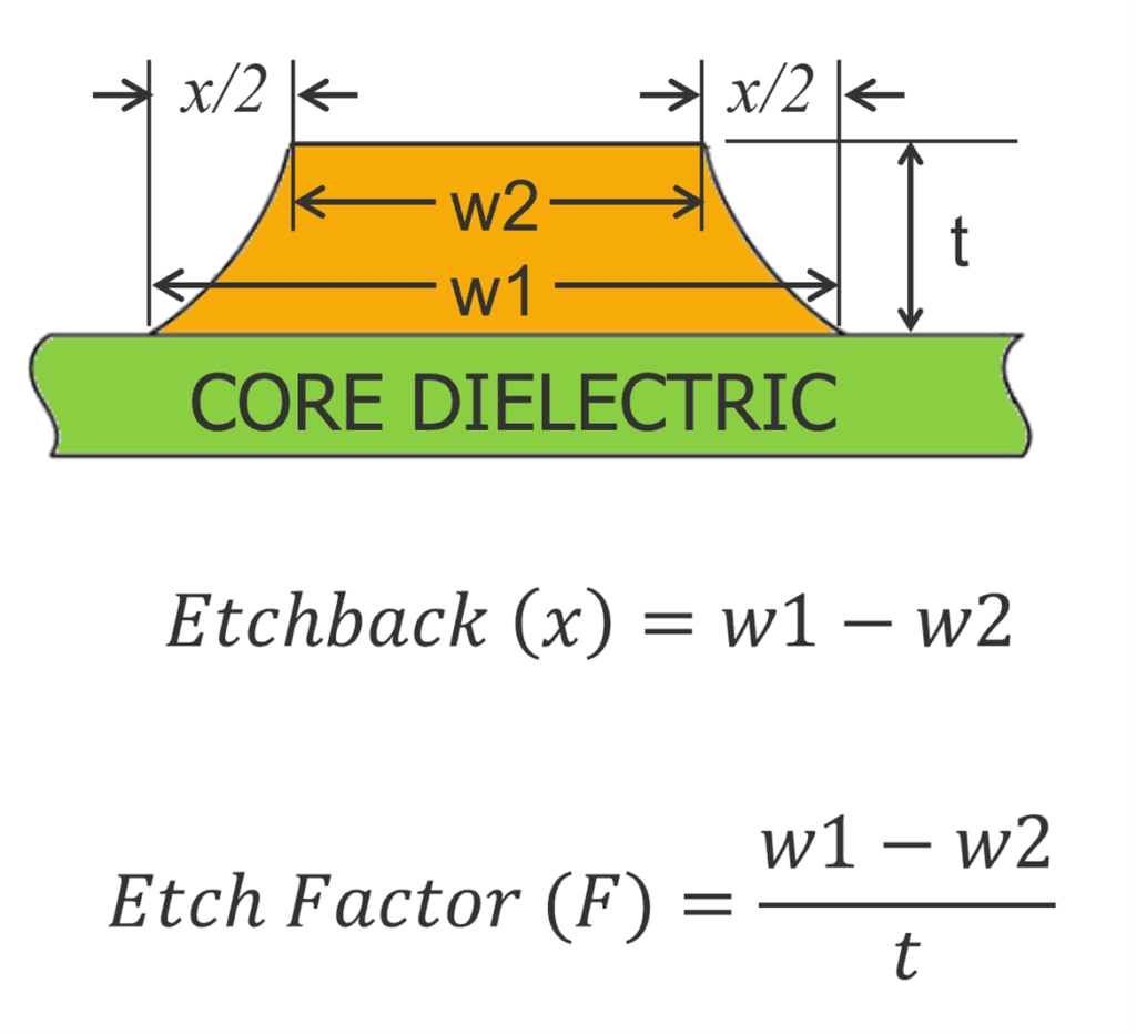
From the parameters in FIGURE 3, there are two descriptive measures of the etching process—undercutting and etch factor. Undercutting is well defined. It’s the average overhang of resist after top width reduction. Hardware teams don’t really need to worry about the width of the resist, but the “undercut” term and concept are useful. Obviously, the goal is to minimize the U parameter.
“Etch factor” is quite a bit murkier. Some define it as being proportional to copper thickness, t, and inversely related to the difference between w1 and w2, the width difference in the trapezoid. But depending on whom you’re talking to, these relationships may be inverted or use different parameters. And even worse, some tools define etch factor as an angle, with values ranging from 45-90 degrees for upward-facing trapezoids and from 270-315 degrees for downward-facing trapezoids. Since industry standards don’t exist, we now live in a world where we need to track and understand how each tool vendor implemented what we all call “etch factor.”
A relationship that I find to be intuitive is shown in FIGURE 5. It would be nice if we could agree on a definition like this, where x (“etchback”) is the difference between w1 and w2, and “etch factor” is defined as the degree of etchback per thickness. This definition is used in HyperLynx, Xpedition, and Z-planner Enterprise.
Fabricator Data
Average suppliers typically maintain roughly 0.25 mils of etchback for half-ounce copper and 0.5 mils of etchback for 1-oz. copper, respectively.
Advanced PCB manufacturers can bring these numbers to 0.17 mils for half-ounce copper and 0.45 mils for 1-ounce copper.
Plated Layers
I hate to open up another can of worms to discuss outer layers, but I will briefly address the subject for completeness. In short, outer layers are even more complicated—particularly when multiple plating steps are used and when copper reduction techniques are used to keep the surface copper thickness down. Sometimes, microstrip traces are anvil shaped rather than trapezoidal shaped, but more commonly they look more like a “mesa,” borrowing a term from geology, with the top plated section almost vertical and then the trapezoidal cross-section at the bottom. (I.e., a rectangle on top of a trapezoid, with the rectangle representing the plated copper.) The Z-planner Enterprise software estimates the cross-sectional area of the plated trapezoid for impedance calculations.
Plated layers often have other challenges, including the fact that there may be 1, 2, or even 3 plating passes. Some designs are plated 1x and end up exactly 1-mil thick, while other boards have 1x plating and are considerably thicker.
Impedance Implications
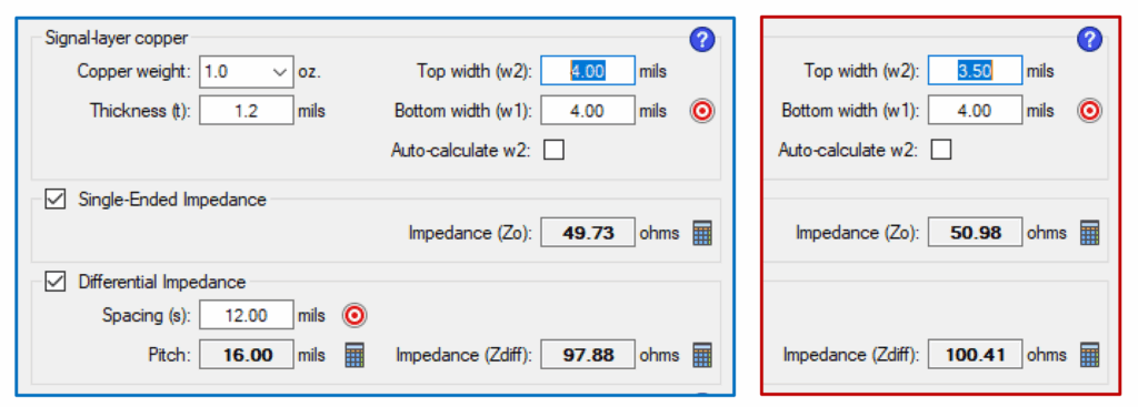
Let’s consider an “average” PCB fabricator, where a 1-oz. stripline layer has 0.5 mils of etchback and compare the impedance results against a trace where etchback is ignored. In FIGURE 6, the left image with the blue border assumes a rectangular trace cross section. The image on the right includes the 0.5 mils of etchback for a single-ended transmission line targeting 50 ohms and a differential pair targeting 100 ohms. As you can see, the single-ended impedance difference is 1.25 ohms and the differential-impedance difference is about 2.5 ohms.
Could your design live with such a difference? It depends on a lot of factors, some that you control and some that are random. You don’t directly control Dk variation or copper-thickness variation from nominal, for example, but you can specify impedance at +/- 10 percent. The difference that we’re showing here would be stacked on top of Dk variation, copper-thickness variation, and any other variation in fabrication. In short, you’re giving up ohms right out of the gate, which is not a good design practice.
Discover more

Go beyond copper etch.
Explore the relationship between copper roughness and signal integrity. Discover 10 critical things you need to know about copper roughness and its impact on board costs during your stackup design process.
Z-planner Enterprise free trial
I would like to encourage your to look into this relationship more yourself. Our free online trial of Z-planner Enterprise has tools which help you to explore and experiment with various trace width values as shown above. The trial grants you full access to the entire suite of stackup design materials, including access to our line of dielectric stackup materials. It provides you the opportunity to perform all of this comparison completely free.