Understanding distribution of current in via arrays
The path of least resistance
We all like to take the path of least resistance. If only it were easier to determine what that path is. How many times have you tried to take a shortcut only to realize it was, in fact, a longer path? And even if you knew the correct path, would you still take it? The beauty of being human is that we get to choose. Electrical current, on the other hand, always takes the path of least resistance. It always knows the path. It does not get to choose. This predictable behavior allows us to simulate the electrical current with satisfying precision, and design electronic devices that work correctly and reliably. Even when the behavior defies our intuition, we can come to realize it is correct, and modify our intuition accordingly.
Expectation vs. reality
One such example which prompts frequent questions from my customers is the distribution of currents in arrays of vias. When connecting power plane shapes on different layers, customers often expect that if they use a very large array of vias, the current will spread out amongst the entire array, and are disappointed to see only a handful of vias in one corner being utilized while the rest sit idly by. Why wouldn’t all the vias be used? It all comes down to the path of least resistance.
Moving through a power plane
The distribution of current in via arrays is determined by the position of the vias more than anything else. Moving through a power plane involves some amount of resistance, and this effect can be visualized by breaking the power plane into “squares.”Because the resistance is proportional to the length divided by the cross-sectional area, if you set width equal to length they will cancel out, and the resistance of a square becomes proportional to the copper weight, or plane thickness.
More precisely, the resistance of that square will be the resistivity divided by the thickness. So, when determining the path of least resistance through a via array, you should realize that including additional vias also requires moving through additional “squares” of plane. In most board designs, that additional square of plane is much more resistive than the via, so the current will be less “inclined” to add that parallel path to reduce the overall resistance. Via connections between planes tend to be short, around 10 mils or so. Even a via going through the entire thickness of the board will have less resistance than moving through a square of plane. As such, the vias are simply there to provide a path between planes, and their position will matter more than anything else.
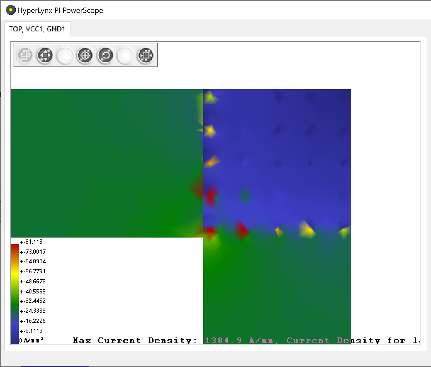
Using DC Drop simulation in HyperLynx Power Integrity
Performing a DC Drop simulation in HyperLynx PI can show how the currents are dividing up in the via array. You can see if you have enough vias. You can see if one via has significantly more current passing through it than the others. You can see the effect of temperature (hint: it’s not as drastic as you might think). You can experiment with vias size, layer span, and, most importantly, the position of the vias to see what effect it has on the division of current. This helps understand the limit of your design, and also helps you design more efficiently for the future. You can get an idea of how many vias are really needed, and how they should be placed. You can eliminate unnecessary additional vias, which not only saves time, but also saves valuable design real estate as well as limits how much the planes are compromised with antipads.
Understanding the paths of least resistance leads to much better designs of your power distribution networks, and much better printed circuit board designs.
If you are interested in learning more about this topic, please read this whitepaper: Distribution of currents in via arrays.


