PCB design best practices: constraint-driven design
The next best practice within the engineering productivity and efficiency pillar is constraint-driven design.
What is constraint-driven design?
Constraint-driven design means designing with the intent of meeting both physical and electrical rules that are defined, established, agreed upon, and then implemented, up front during schematic creation to help ensure the final end-product is designed correct by construction. This will provide the highest potential for meeting all final requirements, and enable you to design quality into the board, governed by these predefined constraints, so that you are not just simply checking if all final requirements were met after the fact.
What’s not working?
Your rules might be inefficient. For example, you may have incorrect trace widths, trace spacing (single-ended and differential), signal trace length matching, class to class rules, component spacing, etc. Another typical problem could be that you have inefficient implementation of the rules that came from your requirements. This usually occurs during both constraint creation, in not defining the rules and net/constraint classes correctly, and or during schematic creation by not assigning the net(s) to the appropriate net classes, constraint class or component grouping/clusters.
What are the roadblocks?
The roadblocks you tend to see are things like time – there isn’t enough time to define, create, and implement constraints. Another roadblock might be that the engineer doesn’t know how to implement constraints because it’s someone else’s role. This ties in one of the biggest roadblocks, which is simply inexperience with the tool.
Best practices: constraint-driven design
The best practice is to implement constraint-driven methodology for PCB design. Then, to create an automated way to manage constraints, so that way you have them structured and standardized in place, but you can also use them repeatedly, design after design – basically by creating and implementing constraint templates. That way you’re not reinventing the wheel on every project. By implementing an existing approved constraint template, all you do is import that constraint template and modify it with whatever new design constraint/requirements are necessary/required for the design at hand. This saves time by using existing data and modifying as needed for a new design.
This constraint-driven design methodology allows you to efficiently and effectively control your electrical or physical rules to meet the final end-product requirements. Then, by creating design constraint templates and implementing them, you increase your potential for success consistently, from design to design, as well as reducing engineering design efforts and costs.
The value you’re going to get from this is the fact that you’re going to design quality into your board, you’re not going to check for it after the fact. With these rules (constraints) in place, you’re going to have confidence knowing that you’re meeting all your end-product requirements during the design process. You’re also going to have an established method that allows you to implement rules more efficiently. And like I said, you eliminate the human factor of having to go back and check your design. It’s an automated design rule checking (DRC) in real-time throughout the entire process, as you’re designing the board. It’s a method of designing PCBs by preventing errors, rather than to have to manually check for errors and correct them after the fact, which is most often too late in the process and can be costly.
How it works: constraint-driven design
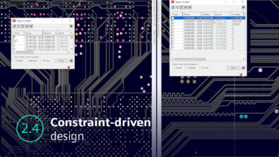
Constraint entry for a design in Xpedition is done, either in the front end (schematic) or backend (layout) in an easy-to-use spreadsheet like GUI, which allows cross probing to the applications like schematic and layout. It also has powerful built-in automation for simplifying tasks such as identifying and assigning differential pairs, to data metrics verification/validation.
These constraints are then available in other areas of Xpedition. Another example is the target lengths dialog that the designers can use, which helps make sure that when tuning nets, they stay within the parameters laid out in the constraint manager, such as minimum and maximum length and tolerance. Designers can utilize tool automation in layout to have the traces tuned by the tool, instead of attempting to do it manually. DRC checking becomes simplified, and the design is ultimately designed correct by construction, leading to the highest potential for success.
To learn more about constraint driven design visit our website or watch this video:


