ABCs of PCBs – M for Manufacturing
Welcome to ABCs of PCBs – a blog series to help new engineers learn about the world of Printed Circuit Boards. I’ll be covering topics from general engineering concepts to PCB design specific rules. As this is a ‘basics’ blog, I’ll keep the content software independent, but any visuals will be from the Mentor PADS Professional PCB suite.
If you missed the last post in this series: ABCs of PCBs – L for Library click here!
So you’ve designed a PCB. The schematic worked out, maybe you did some pre-layout analysis to make sure you had design notes ready to go, and you’ve finished laying out the design. Everything is all set to be manufactured. Although you may send these projects out to manufacturers like PCBWay or 4PCB, it’s good to understand what you can do to make sure manufacturing goes as smoothly as possible.
When it comes to creating a PCB, we’re all looking to optimize product quality while reducing cycle time. When you run into roadblocks prohibiting you from reaching these goals, it’s important to see if these problems are manufacturing or design related. Guessing between the two can cause major setbacks, but manufacturing analysis – commonly referred to as design for manufacturing (DFM) – can aid in pinpointing fabrication and assembly process issues earlier and guide you to resolving them before boards are sent further in the PCB creation process.
You may find fabricators that conduct these manufacturing design checks in house, but you may need to go back and forth with them to make sure these issues are reflected in your design before production. However, you might be able to save valuable time by running DFM checks on your own. Some PCB design software allows you to run DFM checks so you’re prepared and confident that what you send to the manufacturer is right the first time around.
Some of the most common manufacturing issues you may run into are insufficient proximity, annular rings, and slivers.
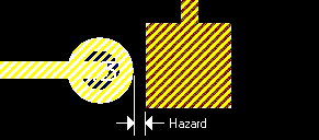
The proximity between traces and other electrical components can become a clear hazard. If pins miss a clearance from a plane layer for example, there’s a chance the pin and plane tie together shorting the signal to the plane.
Annular rings are the remaining ring of copper left after drilling a pad and when designed too small can create some major issues. Pads can delaminate from the board or disconnections can create shorts on the plane.

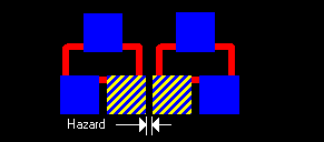
Slivers can be a potential and unexpected hazard when creating boards. Small copper slivers can detach themselves during assembly and accidentally reconnect themselves anywhere on the PCB. This is an area of concern because this can short a net and ruin the entire product.
Historically, DFM checks were primarily done in the fabrication and manufacturing stages. It’s clear, though, that the later a change in the design occurs, the more the total cost increases and the more time it takes to reach a final product. So why not check your designs on your terms before they even reach the manufacturer!
Are you a student? If so, try your hand at designing and testing a PCB with the free PADS Professional Student Edition.
Thanks for reading and see you next time for more on the ABCs of PCBs.
-Shivani Joshi


