PCB Design Using Blind or Buried Vias Could Lower Fabrication Costs
Anytime we consider using fabrication technology outside “the normal” we’re thinking in the back of our minds that – it’ll probably cost more due to extra steps and special processes. In the past, this was likely the case. Today however, the cost of incorporating advanced technologies like flex – which increases product reliability or blind and buried vias that can reduce fabrication cost is more “normal”.
- Flex technology can eliminate connectors and assembly processes.
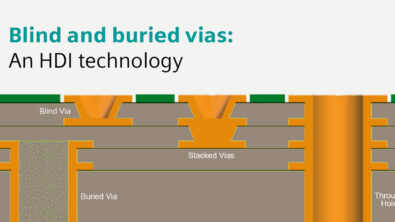
- Adding blind or buried vias can tackle high density and eliminate layers.
If you’re not familiar with these types of vias here’s how they can save on fabrication cost. Let’s use the example of an 8 layer design with a 300 pin BGA. About half the pins on this BGA will be power & ground and about half of those will be ground. Normally these ground pins would need through vias which would congest routing channels under the BGA. If we can simply use a blind via from layer 1 to 2 and another on the bottom for 7 to 8 it would open up routing channels that result in the ability to eliminate 2 layers that would otherwise be required for routing. Removing these 2 layers will save on materials thus reducing fabrication cost. As a bonus, you can reduce grounding noise with reduced inductance for ground vias.
Try PADS Professional Free Today
Before starting your next project consider calling your fabricator and asking questions about their blind and buried via capabilities and how removing 2 layers or more from the design will reduce fabrication costs.
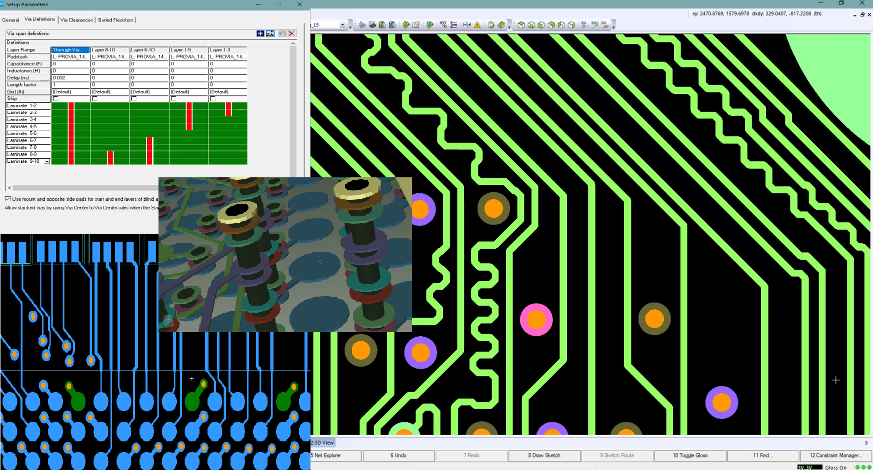
The next question is: Does your PCB tool support, or make it easy or difficult to work with these types of vias? Most tools today support these technologies, but if it’s too difficult to work with or does not work well you may avoid going in this direction unless the cost savings are significant. To learn more about using these technologies watch this new on-demand webinar.
Routing Capabilities You Need to Accelerate PCB Design and Reliability
In addition to blind and buried vias, you’ll learn more about area rules and their advantages along with simple length matching for high-speed nets.
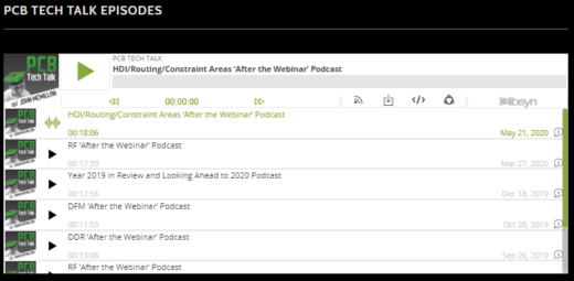
During the webinar, we answered several questions live but there were too many for our allotted time we could not get to all of them. John McMillan and Brent Klingforth put together an “After the Webinar Podcast” with answers to all the questions asked during the 2 live webinar sessions.
Click Here to Listen Now!