ABCs of PCBs – E for Efficiency
Welcome to ABCs of PCBs – a blog series to help new engineers learn about the world of Printed Circuit Boards. I’ll be covering topics from general engineering concepts to PCB design specific rules. As this is a ‘basics’ blog, I’ll keep the content software independent, but any visuals will be from the Mentor PADS Professional PCB suite.
If you missed the last post in this series: ABCs of PCBs – D for DRC click here!
Efficiency is a word we hear over and over. Studying efficiently can allow for less stress and hopefully a good grade on an exam. An efficient budget helps us save and plan for a big spring break vacation. I’ve been seeing more videos on efficient hand washing techniques to help prevent catching/spreading COVID-19. In the same way these efficiencies affect our lives positively, efficient PCB design techniques can help you reach your designs goals the first time around.
Here are some tips and tricks to follow:
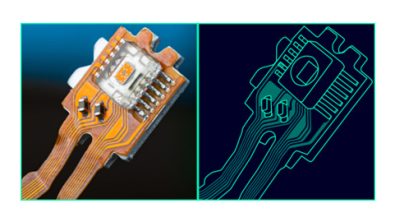
Separate your analog traces –
You want to minimize noise on any trace, but the amount of noise necessary to affect an analog signal is significantly lower than what is required for a digital one. If you’re dealing with high frequency signals, you want to keep them as far away as possible from the traces that can’t afford to accept noise.
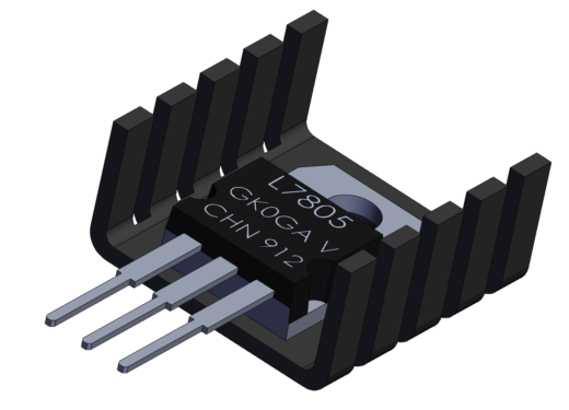
Use a heatsink –
It’s important to note the thermal properties of the parts you plan to use on your board. If transistors get too warm, they could negatively impact your circuit or even fuse. Placing copper around a SMD (surface mount device) or adding metal to a through hole part will help dissipate heat effectively. Remember to account for any extra copper or metal in your design by making sure you’re leaving room for an external heatsink and aren’t adding excessive capacitance.
Use consistent orientation, if possible –
When you’re placing components in layout, try to keep the same orientation in order to eliminate future confusion and avoidable failures. For example, diodes are easy components to rotate and remain visually similar, but a different orientation produces drastically different results. If you keep the position consistent, like + (or anode) is always to the left, then you minimize your chance of making a mistake and possibly blowing your PCB.
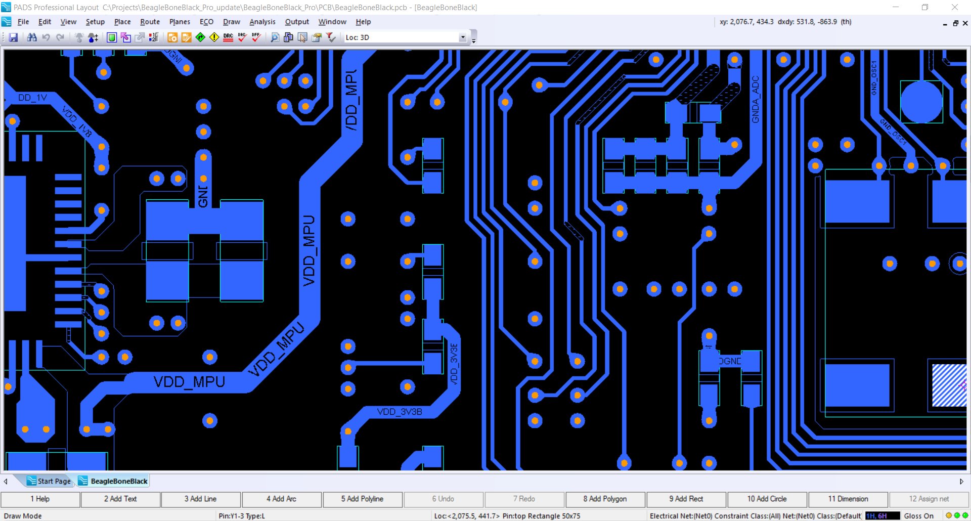
Widen power and ground traces –
Your power and ground traces will have the most current in your design, so you’ll need to accommodate by widening those traces. Although it is possible to keep these traces the same width as your other signal traces, you’ll notice an increase in temperature which can affect the system as a whole. You may see boards with widened ground traces from decoupling capacitors to the outer dimension of a via to account for this type of temperature effect.
As you continue with your designs, you’ll recognize what issues keep reoccurring how to address them proactively. It’s all about taking some time beforehand to do some research and plan. For a good read on the non-technical characteristics of excellent PCB designers, take a look at this white paper.
Thanks for reading and see you next time for more on the ABCs of PCBs.
-Shivani Joshi