Reduce Design Time Using Routing Automation – Part 1
In part one of this two part blog series, we will look at how intelligent routing can assist in creating fanouts, design rules, and sketch routing for multi-trace routing. The second part of this series will examine more advanced routing automation such as sketch routing for differential pairs, interactive trace tuning and dynamic and ground planes for large spacing.
Introduction: Why is Routing Automation important?
Automated intelligent PCB placement and routing can accelerate design cycle times up to 50% or more, eliminating issues due to collision and space constraints. Designers are three times more likely to achieve first past design success and produce quality board designs on time using intelligent automation offered in PADS Professional.
The fact is, many PCB design projects miss schedule commitments by 70% due to delayed routing and lack of automation. Moreover, due to late stage design changes, schedules are not met and the addition of those new items takes 10 times or longer to incorporate than if changes were added from the beginning.
Over the past several years, powerful routing capabilities have been added that allow the designer to address specific, critical tasks. Some of these routing capabilities include fanout for power, grounds and signals, sketch routing, interactive signal and multi-trace routing, dynamic planes, interactive trace tuning, via stitching, auto creation of differential pairs and design rule reuse. PADS Professional is a leader in the industry providing all these capabilities, combined with many other automation features, helping to reduce design time while improving quality.
In this first of two blogs, we will look at how intelligent routing can assist in creating fanouts, design rules, and sketch routing for multi-trace routing. The second part of this series will examine more advanced routing automation such as sketch routing for differential pairs, interactive trace tuning and dynamic and ground planes for large spacing.
Fanouts for Power, Grounds and Signals
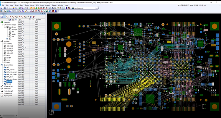
PADS Professional provides a separate window for components and net-exploring that divides into several sections including: net classes, constraint classes and user groups, plus specifically defined groups of nets like differential pairs. In the constraint editor system, items in the defined constraints—either in the schematic or in the PCB layout—are automatically transferred and viewable. The PCB designer has the ability to cross probe back into the workspace.
The first task in routing the PCB is typically to create the fanouts for components. The designer can select a component and the tool will automatically fanout the part. PADS Professional automates the entire process, saving a lot of time for the designer.
The designer can also create manual fanouts for components and then copy and paste them to other components. Once they are satisfied with the critical fanouts, the designer can select those parts and apply a regular fanout to the rest of the components. PADS Professional intelligently use automation to assist with the design process.
Design Rules
Design rules are a critical function in streamline PCB routing. This can be done either from the schematic or the PCB layout in PADS Professional. For example, designers can create differential pairs with the help of automation that assists the designer throughout the process. Using the auto-assign differential pair dialogue box, the designer can type in the suffix for the nets and click on ‘apply.’ This will display all the nets and create the differential pairs automatically.
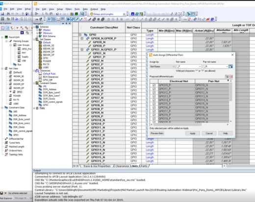
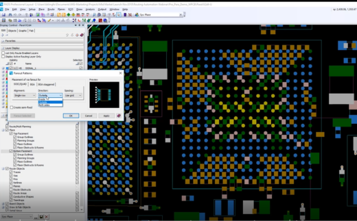
Then, using filtering capabilities in the constraint system, specific rules for differential pairs can be viewed and quickly modified to guide the creation of differential pairs. Once these rules are created, they show up in the net explorer in the layout tool. Another important capability for automating routing of a PCB is being able to create area rules around components. This is critical for designers working with BGAs, power supplies, or analog circuits. Multiple area rule definitions may be needed for different spacing requirements on a PCB. In most tools this is a very complex task, but with PADS Professional it is straightforward and easy to do.
For example, the designer might want to define specific design rules that allow two traces between every via, allowing for more area to route differential pairs. First they would create and name a scheme with the desired design rules that meet their spacing requirements. Once the design has the clearance set and the net classes defined, they then can use a matrix to define what clearance sets are to be used between individual net classes. This powerful function for design-rule creation eliminates time spent replicating design rules over and over again. Basically the rules are defined once and then can be shared between individual classes.
Sketch Routing for Multi-trace
Now that the rules are defined, the next step is the actual routing, which is historically the most time intensive portion of creating a PCB. PADS Professional offers an intelligent level of automation, called interactive routing or sketch routing, to assist the designer in achieving an optimal result in the most efficient manner. There are two methods of sketch routing, called packed and unpacked. Packed uses a draw sketch function where the designer can draw a line across the screen. They can change layers and use different via patterns and the tool will automatically route the nets just as if the designer had hand routed each of them individually. With the unpacked approach, the traces are more spread out and distinct from each other, occupying more area on the board.
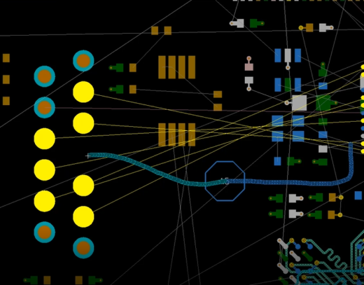
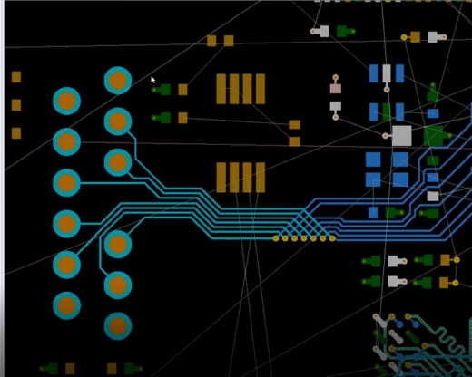
The advantage of sketch routing is that the designer can very quickly look at alternative routing possibilities. The routing is performed so quickly that they can explore different scenarios to find the best layout for the design. For example, a designer could try a horizontal via pattern, but might find that it makes the routes go between components. They could then try adding a constraint that guides the tool to route in a serial fashion, instead of dropping vias and doubling back on itself. If that does not produce the desired result, the designer could try yet another approach, until the desired result is achieved. . At this point, if any nets remain unrouted the designer can individually route the remaining traces using a ‘push and shove’ capability to clean up the final details.
Check back soon for part 2 of this series on intelligent routing.
To learn more about the features and capabilities described in this blog series, check out the routing automation webinar available On-Demand!
Thanks, Brent