Six reasons not to be intimidated by PCB design constraints
As PCBs increase in complexity and density, a higher percentage of the design must be implemented with strict adherence to design rules. Manual documentation and interpretation of design rules is tedious and often results in longer product development cycles.
The constraint manager in PADS Professional provides a fully integrated, constraint-driven design methodology that reduces design costs and time-to-market by automating design rules communication and eliminating unnecessary PCB prototypes and re-spins. Check out this web seminar about “Dealing with dense, highly constrained designs in PADS Professional.”
Here are six reasons why constraints are manageable in PADS Professional:
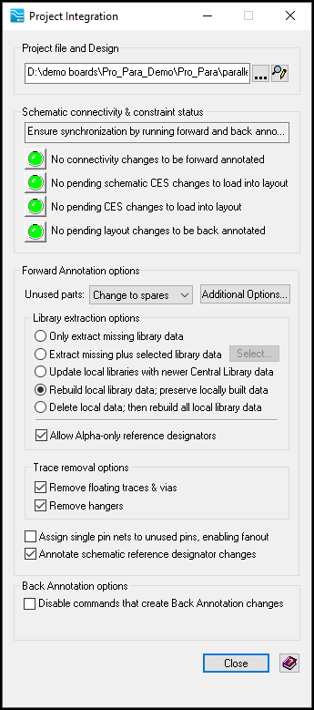
- Constraint integration throughout the design flow: Easy and seamless synchronization with bidirectional cross probing and highlighting between the schematic entry tool, constraint manager, and layout makes maintaining constraints easy and effortless.
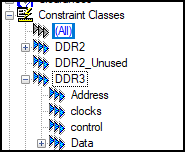
- Hierarchical Rule Classes: You can create rule hierarchy where classes inherit some rules from other classes above their hierarchy. For example, you can have subclasses like “DDR3_Data,” “DDR3_Address,” etc. that inherit rules from the “DDR3” constraint class. This increases the speed and efficiency of constraint entry for complex rules.
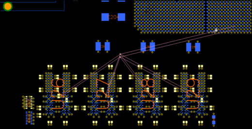
- Topology Assignment: You can create a topology using a virtual pin. You can also use pre-defined topologies such as Chained, H Tree, and Star (as shown in the picture below), as well as user-defined topologies like custom and complex topologies.
- Net Class Schemes: Schemes allow you to have area-specific manufacturing constraints, which override design-wide or layer-specific constraints. These include constraints such as widths and clearances which may have to be modified, for example, around a Ball Grid Array device.
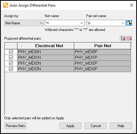
- Automatic Differential Pair Creation: Differential pairs are becoming very common in modern designs. With this utility you can easily assign nets as differential pairs by using wildcard searches on net names and interactive pair selection across the entire design.
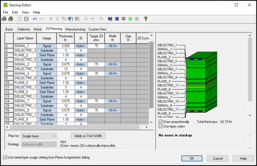
- Impedance Planning: You can view or modify the stackup properties. Users can verify various properties like differential pair impedance, metal type, etc.
Don’t be intimidated by ever-more stringent constraints on your design, ask for an evaluation of PADS Professional and take a look for yourself.