Understanding the DDR memory bus
 In the first blog in my series about DDR design, I talked about the stress of dealing with DDR. To give you a solid footing for our following discussions, let’s get down to the basics of the bus itself.
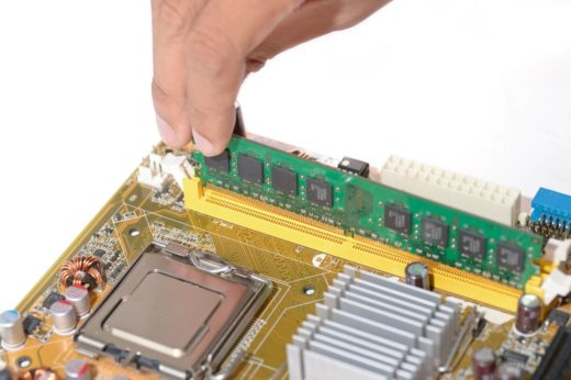
The DDR memory bus is used to send data back and forth between the controller and the DRAM memory chips. The controller is the primary agent that uses the data, writes data to the memory, and reads from the memory as needed. It also bears the burden of the larger system’s functionality. The DRAM, on the other hand, has only one purpose: to store data and deliver it when requested by the controller.
Many of the complexities and IC design decisions of the controller and the DRAM can be explained by the functionality described above.
The controller, with its larger capability set, usually contains a greater degree of functionality and is, therefore, usually more expensive than the DRAM. The DRAMs are usually more price sensitive since the DRAMs need to fit into a vast array of products. This leads them to take on the responsibility of as little functionality as possible in order to reduce costs.
With this in mind, let’s next talk about the signals connecting the controller and the DRAMs – the “DDR Memory Bus.”
The memory bus consists of two large groups of signals: the address/command set of signals (the “address” bus) and the data signals (the “data bus” or “DQ bus”). The address bus sends commands and instructions from the controller to the DRAM. Since these commands are always issued by the controller to the DRAM, the memory bus is uni-directional with the controller always driving, and the DRAMs always receiving.
The bus is synchronized to the Clock (CLK) signals, with the signals on the address bus being sampled by the DRAMs on the rising edge of the CLK signal for all DDR memories (some DDR flavors, such as LPDDR and other flavors might have exceptions where they clock in the address bus on both the rising and falling edges).
From a PCB layout perspective, it is important to make sure that the characteristics of all the signals on the address bus are similar to each other. This means that it would be ideal to length-match all the address signals with the clock, and also with each other. It is similarly desirable to route all the address bus signals on the same layers. Of course, the actual requirements may depend on the capabilities of the controller, so go by the layout guidelines of the controller datasheet for details.
In my next blog, we will continue with the data bus. You can also read about it in my article, ‘Designing PCBs for DDR Busses.’
Comments
Leave a Reply
You must be logged in to post a comment.
Great article. I would like to see if you can dedicate a separate article to discussion how to deal effectively with the high loading affects of Address/ CLK buses
That’s indeed a troublesome area, Alex. Thanks for the idea for an article.
In the meantime, I’d recommend you use a simulation tool (such as HyperLynx) and try out different topologies and different termination schemes if you have multiple ranks. WIth complex loading, it’s often difficult to come up with an ideal simulation purely through intuition. Simulation is often a great aid to hone in on the appropriate solution.