3D PCB Design – Far from Flat
In my placement blog series I talked about the old days when we as PCB designers used “paper dolls” to mimic footprint placement. Feeling nostalgic, I think back again to my days at Rockwell International (you now know them as Boeing), and my first introduction to 3D design in the printed circuit board industry.
Being the young whipper-snapper that I was, I never considered the manufacturing issues that could occur during the assembly phase of any of my designs. My mentor at Rockwell International, Frank Caster, was an engineer and after my first layout placement for a Peacekeeper Missile Program design, he schooled me on the need to verify that the placement would work with the overall system design. I had no idea what he was talking about!
Frank asked me to follow him to a lab with a security guard at the door and a combination lock on the door. Upon entry to the lab, I got my first look at a portion of stage IV of the Peacekeeper missile, called the Missile Guidance Computer System (MGCS).
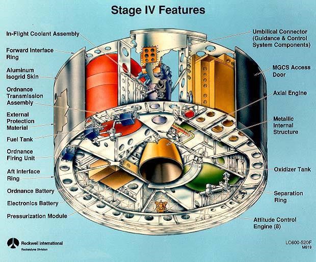
My PCB design was just one of the over 20 boards that made up the MGCS. Frank told me, “Vern, the world is not flat and neither is your PCB!” He explained that my board had to fit into one of the slots in the chassis I was looking at and that it could not interfere with any of the other cards within the chassis. The cards would have to be able to be maintained for years, and it would not be good if parts were knocked off the other boards when cards were replaced.
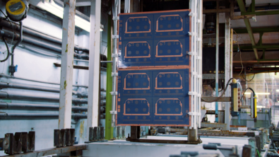
I was then shown a mockup of the MGCS and some lab technicians that were using X-ACTO blades to cut tiny 1:1 scale PCB components out of foam board. They were making a mockup of my design placement, completely to scale, that they could fit into the chassis with other scale cards in order to make interference measurements – a process that I was told took an extremely long time.
A light came on, and a bell rang in my head. I now understood that just because my design worked for me, it did not mean that it would work for everyone else!
In essence, every PCB we design has to go somewhere else. Whether it is an intricate missile guidance chassis, or a simple box, it has to fit perfectly into the full system.
Fortunately today, we have powerful computers that allow us to create 3D models to check mechanical measurements within our designs. But, until recently these systems had to be run by highly trained mechanical engineers. The PCB guys were at the mercy of another process to let them know if their designs would work.
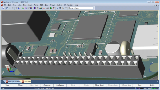
But NOT ANYMORE! Xpedition is now available with integrated 2D and 3D layout, and the power of 3D has been put into the hands of the PCB design engineer.
Take a look at this video, 3D Layout with Photo-realistic Visualization, and see how 3D layout helps you visualize and validate your design as if it were already manufactured.
In my next post, we will discuss the new world of integrated 3D PCB layout.