Feeling suppressed? Hopefully your radiated emissions are.
This is the second in a three-part series discussing PCB design EMI reduction.
In my previous blog post, I discussed different methods of containing radiated emissions. However, containment is a really poor solution to the problem. A better solution is to suppress emissions by fixing the problem areas on your board.

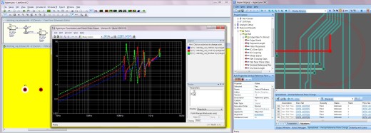
HyperLynx DRC can find a number of structures that can cause unwanted emissions from a PCB, most of which involve poor or missing return paths. I have blogged many times in the past about the importance of return path. Breaks in return path can come from something obvious like a trace crossing a plane split, or something a little less obvious like a signal via, or even a signal going through a connector.
Care must be taken to make sure that the signal return path stays continuous throughout its path along the board, which may be accomplished with something as simple as intelligent layer selection, or as complicated as adding stitching vias and capacitors. I discuss this in greater detail in “Options for Reducing EMI on a PCB Design,” my recent article on Printed Circuit Design & Fab.
If you aren’t yet sold on the importance of return path for high-speed signaling, try disconnecting the shield on your cable TV cable, and you will probably start feeling a little suppressed…


