Simultaneously Switching Noise: the Effect of the Power Distribution Network
This is the second post in a three part series that will examine the problem of SSN and explore methods of reducing SSN in your designs. Click here to read part 1.
In the first installment of our blog series on Simultaneously Switching Noise, we went through an overview of SSN and explained its relevance to high-speed parallel busses such as DDR4. This time, we’ll be taking a closer look at the effects of a poorly designed Power Distribution Network (PDN) on SSN and signal integrity.
Effects of a poorly designed PDN
To illustrate the effects that a PDN can have on signals, consider a setup of a single DDR4 byte lane running at 2400Mt/s with each signal running a unique random sequence. In this simulation setup, the package capacitor is not loaded. This removal of a major source of power for the higher frequency transitions (artificially) exacerbates the SSN effect.
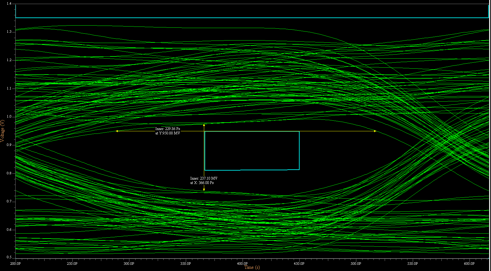
In Figure 1 above, the eye for DQ0 does not have a lot of margin around the eye mask. This is not a very good situation.
Bad PDN: Worst-Case Switching
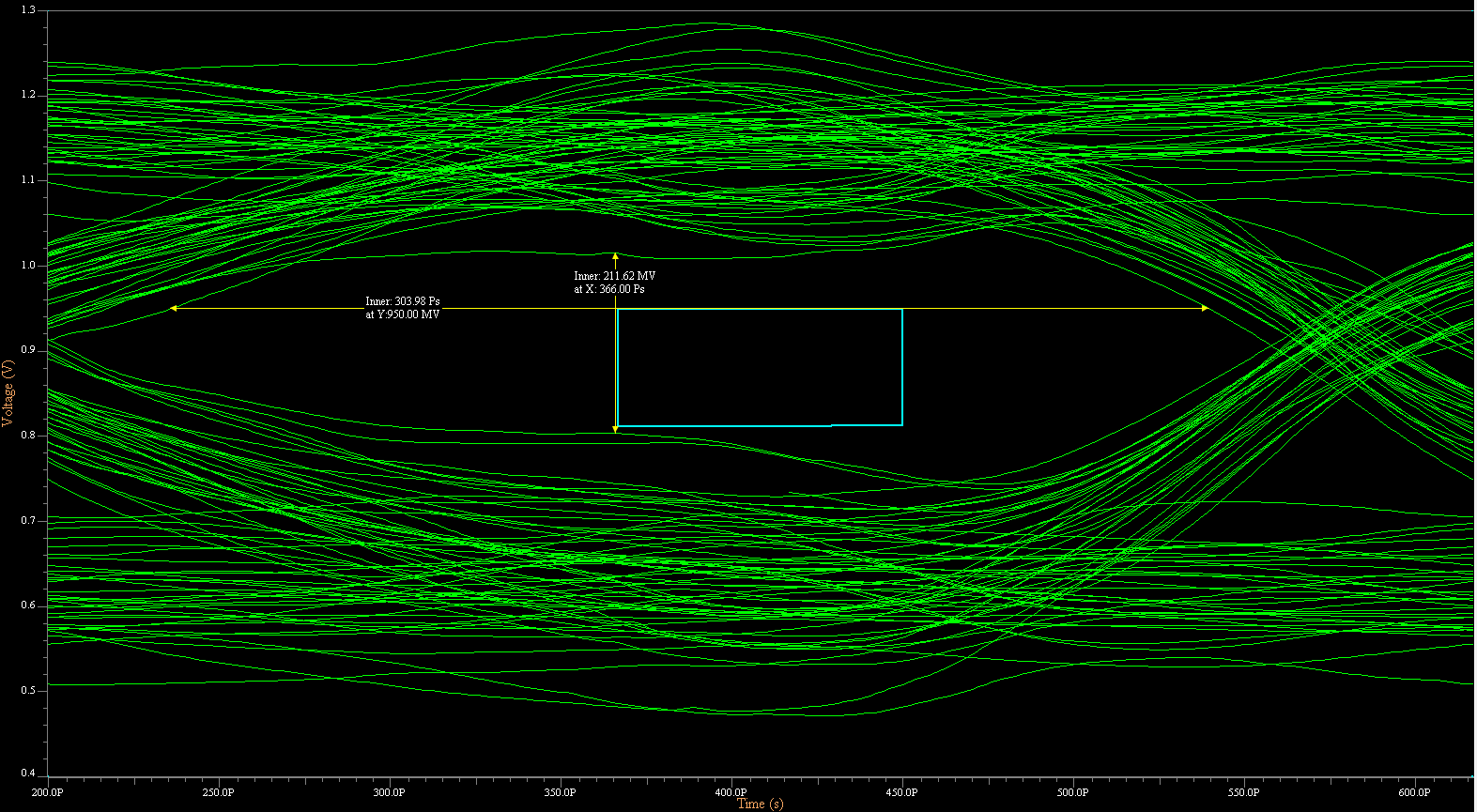
We can see the situation get worse if instead of allowing each signal to have a unique random sequence, they all switched with the same sequence. This way, we can see the worst-case effects of SSN—that is, when all the signals are toggling in unison and placing a great deal of strain on the voltage rail.

As can be seen in Figure 2, the eye for DQ0 gets a whole lot worse if all the bits are toggling with the same data pattern. In this case, this causes the eye to get closed.
Improving the PDN
Next, let’s insert the 4.7uF package capacitance which was removed to begin with. This should be a low-ESR capacitor and should be placed so that the inductance-causing loop area is minimized.
In this setup, all the signals continue to toggle with the same bit-pattern. So, this is the worst-case situation with the package capacitor inserted. This DQ0 waveform in Figure 3, while better than that generated without the package capacitor in Figure 2, is only barely passing the eye mask.
In a more realistic situation, the signals would indeed be independent of each other. Using unique random bitstream for each signal, we get the DQ0 eye shown in Figure 4.

The DQ0 eye improves dramatically. The smallest eye height in the mask region is now 275.5mV, better than the 211mV eye-height in the setup with the package capacitor where all the signals switch identically (Figure 3) and better than the 237mV eye-height with the setup where the package capacitors have been removed but the signals toggle independently of each other (Figure 1).
What we can gather from the above data is that the eye can be improved by adding appropriate package capacitors, or by ensuring that signals don’t all toggle identically. Ensuring that all the signals don’t toggle identically is one of the benefits of enabling the Data Bus Inversion (DBI) option in DDR4.
We will conclude the blog series next week by speaking more on the DBI option in DDR4. In the meantime, if you’d like to learn more about SSN and similar challenges, check out our white paper “DDR4 Board Design and Signal Integrity Challenges,” which was recently nominated for a DesignCon Best Paper Award.
Click here to read part 3 of this 3 part blog series.