Simultaneously Switching Noise: An Overview
This is the first post in a three part series that will examine the problem of SSN and explore methods of reducing SSN in your designs.
Digital designers have become accustomed to signal noise coming in from all directions. With the data rates running on the faster parallel busses, designers will now also need to be concerned about the noise coming out from the chip itself. One such kind of noise, Simultaneously Switching Noise (SSN), occurs due to the Simultaneously Switching Output (SSO) of buffers on a driving chip.
What causes SSN?
When a driven signal inside the chip transitions states, it consumes power from the rail. If a sufficient number of signals switch simultaneously, the rail might droop due to an inadequate access to immediately-required charge to provide current for all the switching outputs. This could happen because the capacitors from the Power Distribution Network (PDN), which are providing the charge, are too far away, or because those capacitors have been laid out in a way which causes them to have a high series inductance.
Subsequently, this droop in rail voltage causes the drivers to not drive clean signals. This is similar to crosstalk-induced noise in that the switching of one signal can cause variations in the output of another signal.
Accurately simulating the current draw of one driven signal on the voltage rail and the subsequent effect on other drivers requires information regarding the buffers’ behavior. One option would be to use Spice models. Alternatively, IBIS allows simulations which are much faster than Spice at a comparable level of accuracy, and is therefore a popular standard for simulation. IBIS 5.0 supports the data structures needed to simulate this “power-aware” topology.
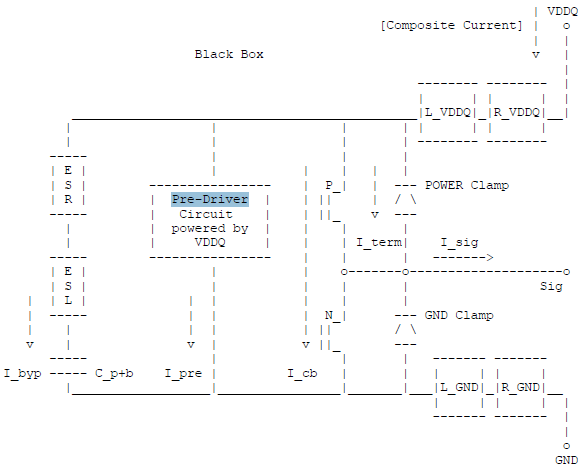
SSN is particularly relevant to high-speed parallel busses such as DDR4. With parallel busses, each bit can act independently of the others. This can cause greater loads on the power rails when the signals all switch in unison, creating a greater load on the rail.
In the second installment of this blog series, we’ll take a look at the effects of a poorly designed PDN on SSN and signal integrity. In the meantime, if you’d like to learn more about SSN and similar challenges, check out our white paper “DDR4 Board Design and Signal Integrity Challenges,” which was recently nominated for the DesignCon Best Paper Award.
Click here to read part 2 of this 3 part blog series.


Comments
Leave a Reply
You must be logged in to post a comment.
what is the max frequency range can do SI analysis in latest version?
The capability of the tool depends on the accuracy of the setup. At DesignCon 2016, we showcased a measurement correlation at 25GT/s. The tool can be used at much higher data rates with careful design.