7 PCB SILKSCREEN QUICK TIPS – White paper
Today, it’s hard to imagine a GPS that doesn’t list landmarks, street names, or even exit numbers. Every bit of visual information we can get from map symbols and text makes navigating easier and faster. The same is true for a PCB, yet we often overlook a great opportunity to provide a wealth of information about our PCB’s design on the silkscreen. The information we can, and should, supply on PCB silkscreens should go beyond component outlines, reference designators, and pin 1 indicators.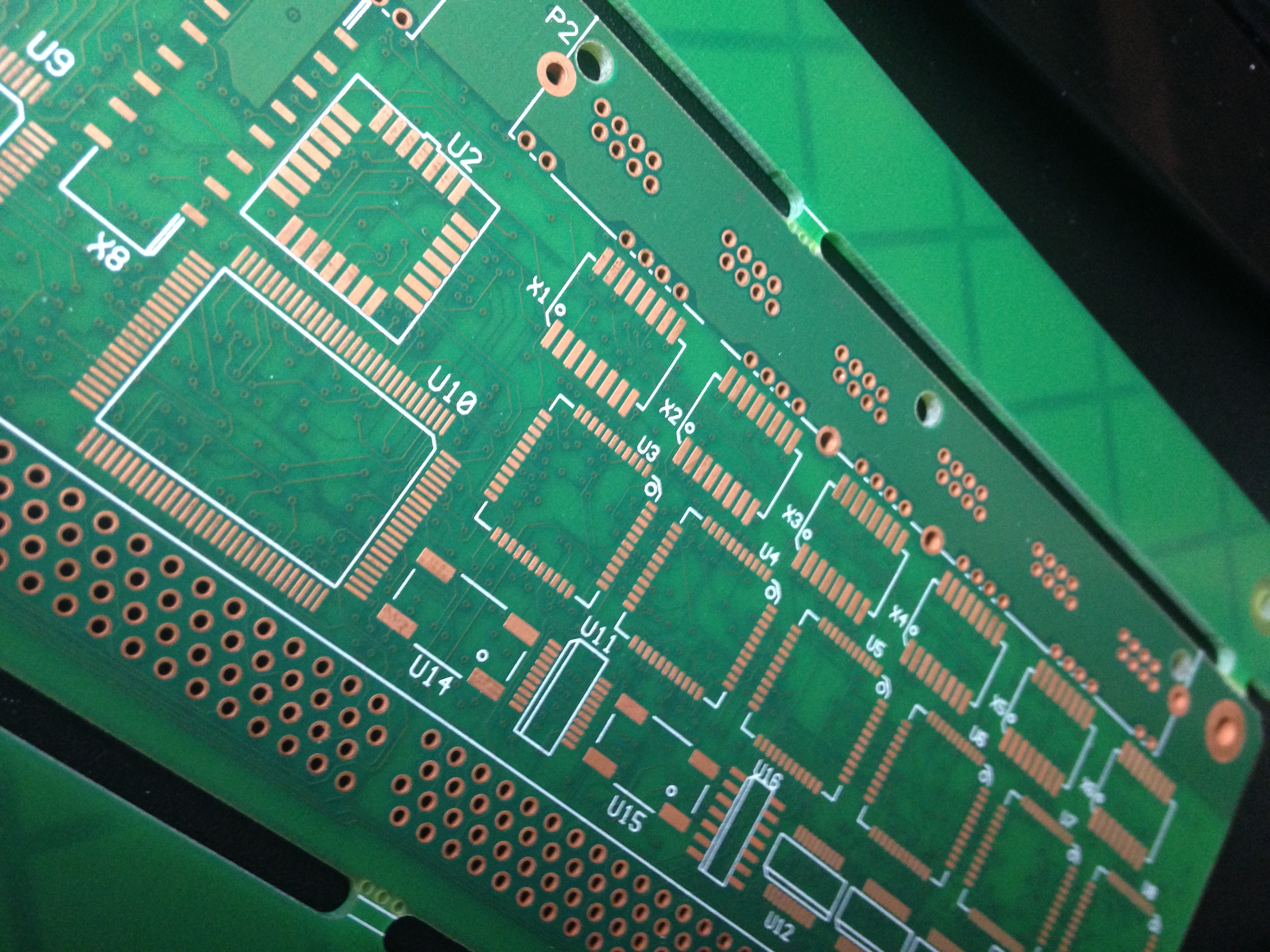
In this white paper I’ll describe and display some of the enhancements you can make to your PCB designs’ silkscreens that can add value at both the bare board and assembly levels and from the test bench to the installation.
Silkscreen items covered in this paper include:
- CONNECTOR ANNOTATIONS
- MULTI-LEAD COMPONENT ANNOTATIONS
- POLARITY ANNOTATIONS, THOSE PESKY DIODES
- PHYSICAL INTERFACE COMPONENT LABELS AND ANNOTATIONS
- REFERENCE DESIGNATOR ANNOTATIONS
- TEST POINT ANNOTATIONS
- DFM ANALYSIS CHECKS FOR SILKSCREEN ANNOTATIONS
I’m looking forward to hearing from you about the different ways that you’ve taken your PCB silkscreens from ordinary to extraordinary!
Thanks for reading,
John