Solving the extraction challenges of CFET and backside power
By Karen Chow, Sheetal Veronica, and Kunjesh Agashiwala
Introduction: The vertical evolution of semiconductor architecture
Both complementary field-effect transistor (CFET) technology and buried power rails (BPRs) for backside power delivery network (BSPDN) are important technologies for very advanced semiconductor chips, such as 3 nm and smaller.
A CFET or complementary field-effect transistor, is a new kind of tiny switch used inside computer chips. For many years, engineers made chips better by making transistors smaller and squeezing more of them onto a chip. But now transistors are already super tiny and it is harder to fit more transistors on the chip, keep them from wasting energy, stop them from overheating and make sure they work reliably. Instead of spreading transistors out flat like houses in a neighborhood, CFETs stack them upward like floors in a skyscraper (figure 1). They stack the two important transistor type, n-type and p-type, together in one 3D structure. This can reduce the space needed for some transistor layouts by up to about half, which is a huge improvement in chip design.
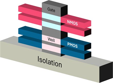
Figure 1. A complementary field-effect transistor (CFET) stacks an n-type device over a p-type device to save space.
A buried power rail (BPR) is a chip design technique where the power supply lines are placed inside the silicon substrate – underneath the transistors – instead of being routed mostly on the top metal layers of the chip. Then the power can be routed on the back side of the chip (figure 2).

Figure 2. With a backside power deliver network, the power and ground nets are on the back side of the chip and connected to device and the front of the chip through buried power rails and nano-TSVs.
Together, these technologies reduce the chip area needed, improve power efficiency and help meet the high-performance needs of applications like AI accelerators, data centers and mobile processors.
As chip designs become more complex, engineers need very accurate analysis of unwanted resistance and capacitance in these structures. Siemens Calibre xACT helps with this by supporting CFET modeling, extraction for both frontside and backside metal layers, as well as interfaces, through-silicon vias and complex routing patterns.
This helps engineers improve their designs and meet the power, performance and scaling requirements of next-generation electronics.
The chip industry’s vertical leap: Why CFETs are the most exciting — and difficult — transistor breakthrough in decades
For decades, the semiconductor industry has sustained exponential growth by relentlessly shrinking transistors, packing ever more onto a single chip to deliver faster, more efficient computing. But now we are limited by physics: Short-channel effects, quantum leakage currents and extreme heat density have pushed traditional planar designs to their limits, forcing engineers to think in a new dimension literally.
Stacking the deck
Enter the CFET. Rather than placing n-type and p-type transistors side by side as in conventional CMOS designs, CFETs stack them vertically — one on top of the other. This bold architectural leap, first formally described in IEEE literature as early as 2018, enables unprecedented device density without requiring the transistor components themselves to shrink further. It is an evolution of GAA nanosheet technology, taking the 3D transistor revolution to its next logical step.
In a GAA device, the gate wraps entirely around the channel, giving engineers far better electrostatic control. CFETs take that architecture and go further — stacking an entire NFET on top of an PFET within the same cell footprint (figure 3). The result is unprecedented device density at nodes that would have seemed impossible just a few years ago.

Figure 3. In a GAA device, the gate wraps entirely around the channel and the n channel and the p channel are side by side, whereas in a CFET device, the gate still wraps around, but the n channel is on top of the p channel.
Two manufacturing approaches are being explored: The monolithic approach grows both transistor layers together in one continuous process. It offers better alignment, lower cost and superior performance – but it demands high aspect ratio (HAR) etching with almost impossibly tight tolerances. The sequential approach, on the other hand, fabricates the NFET and PFET separately before bonding them together, which opens the door to using different channel materials for each layer. The trade-off here is the need to have near-perfect vertical alignment between the two and thermal budget is a critical constraint in the sequential integration approach. In either case, miss the process window by a few nanometers and you’re looking at unintended shorts or opens – an inoperable device.
The extraction problem nobody talks about
Here’s where things get interesting – and where most public coverage of CFETs falls short.
Building the transistor is one challenge. Accurately modeling what you’ve built is another one entirely.
Every physical structure in an IC introduces parasitic resistance and capacitance – tiny, unintended electrical effects that arise from the geometry of the device itself. At mature nodes, parasitic extraction was complex but manageable. At the dimensions CFETs operate, parasitics can dominate device behavior. A small error in modeling the resistance of a buried power rail contact or the capacitance between stacked metal layers, can cascade into performance failures, timing violations or reliability issues that only show up after tape-out.
CFETs introduce new extraction challenged that existing EDA tools were never designed to handle. The vertical stacking of NFET and PFET means you now have frontside and backside metal stacks that interact with each other in complex ways. Backside power delivery networks use through-silicon vias (TSVs) and non-Manhattan routing – diagonal or curved metal paths that standard extraction engines weren’t built to model accurately. Interface resistance between bonded layers, coupling effects between TSVs and the RLCK parameters of the entire structure all need to be captured with high fidelity before a single chip is manufactured.
This is the challenge that Siemens EDA’s Siemens Calibre xACT platform is designed to address. By providing unified extraction workflows that span both front and back metal stacks and by incorporating models for TSV coupling and non-standard routing geometries, tools like this are becoming as critical to CFET development as the fabrication process itself. Design verification at this level isn’t a nice-to-have – it’s the difference between a chip that works and one that doesn’t.
Power from below
CFETs don’t work in isolation. One of the most critical co-developments enabling this architecture is the buried power rail (BPR). Traditional chips route their power networks across the front side of the die, which is convenient but ends up consuming valuable routing resources and adds resistance. BPRs flip the scenario by embedding the power delivery network directly into the silicon substrate, below the transistor layer.
The result is a chip where the front side is freed up for signal routing, power delivery is more efficient and the overall area footprint shrinks further. When CFETs and BPRs are designed together, you get a compounding benefit: denser logic, cleaner routing and lower power consumption. It’s not just an incremental improvement – it’s rethinking how the entire chip is organized.
This combination is already being targeted at some of the most demanding applications in computing: AI accelerators that need to process staggering amounts of data with minimal energy, data center chips that run around the clock under brutal thermal loads and mobile processors where every milliwatt matters.
Why this matters right now
CFETs aren’t shipping in consumer devices today. But the groundwork being laid — in research labs, EDA tools and process development — will determine what chips look like in 2028 and beyond. The companies and teams that solve the extraction problem, nail the fabrication tolerances and develop robust design flows for CFET architectures will have a decisive advantage in the next generation of semiconductor leadership.
For years, we scaled by making things smaller. The next chapter is about making things smarter – and taller. CFETs are the clearest signal yet that the industry isn’t out of ideas. It’s just starting to build in a new direction.
Backside power delivery scheme and its relevance for sub-2 nm technology nodes
As CMOS scaling progresses toward the sub‑2 nm regime, the key limiter to performance and energy efficiency is no longer transistor electrostatics alone, but power delivery integrity. In conventional frontside power delivery networks, power and signal wires compete within the same back‑end‑of‑line (BEOL) stack. Advanced designs may require 15–20 metal layers to deliver current from package bumps to the standard-cell rails, resulting in excessive IR drop, routing congestion and electromigration constraints.
At technology nodes below 2 nm, power interconnects can consume 20–30% of total routing resources, significantly limiting logic density and timing closure. Backside power delivery networks address this limitation by relocating the power grid to the backside of the wafer, thereby fully decoupling power and signal routing. Backside power delivery involves three fundamental process innovations:
- Wafer thinning to expose silicon suitable for backside metallization
- Backside metal stacks optimized for low-resistance power rails
- Vertical interconnects (nano-TSVs or direct contacts) linking backside power rails to frontside devices
These process innovations enable thicker, wider power metals unconstrained by signal pitch, higher decoupling capacitance and improved reliability margins, thereby representing the larges architectural change since FinFET adoption, redefining power integrity strategies for the next decade.
Buried power rail technology
BPR technology relocates the VDD and VSS rails from conventional BEOL metal layers into the front‑end‑of‑line (FEOL) or middle‑of‑line (MOL) region, embedding them below the transistor channels. These rails are typically formed by etched trenches filled with metal and dielectrics before device fabrication completes. Unlike backside power delivery networks, BPR operates at the standard‑cell level, directly affecting cell architecture, height and routing. Furthermore, BPR eliminates the need for top‑side rails, enabling aggressive cell-height reduction and freeing first‑metal layers exclusively for signal routing.
Experimental and design-technology co-optimization (DTCO) studies at IMEC and various academic institutions show that BPR provides
- ~25-85% reduction in on-chip IR drop
- ~10-20% reduction in internal power consumption
- Significant time and delay improvements
- Up to 75% standard-cell area scaling relative to older nodes
While the BPR and backside power delivery scheme present significant upgrades in the overall chip power. Performance and area (PPA) metric, several design and manufacturing challenges remain, mostly related to:
- Precise overlay alignment to devices
- Stress and thermal management near channels
- Defect detection in buried metals
- New extraction and parasitic modeling flows
Despite these issues, BPR has become a baseline assumption for sub-3 nm logic design.
Calibre xACT, Calibre xACT 3D and Calibre xL for CFET and backside power delivery
Both CFET and backside power delivery improve density and performance potential, but they make parasitic resistance, capacitance and inductance extraction significantly more complex.
In advanced nodes, parasitics are no longer small “layout side effects.” They can dominate delay, power, signal integrity and reliability.
Calibre xACT, Calibre xACT 3D and Calibre xL fully support both CFET and backside power delivery.
In CFET, nFET and pFET devices are placed on top of each other rather than side by side. This creates a highly three-dimensional electrical environment.
Key parasitic concerns include:
- Gate-to-gate coupling between stacked devices
- Source/drain-to-source/drain coupling across vertical layers
- Gate-to-source/drain fringe capacitance
- Coupling through intermediate dielectric layers
- Coupling between local interconnects above and below the device stack
Siemens works closely with the foundries to make sure that the boundary between device models and parasitics are correctly handled.
Backside power delivery, parasitic extraction challenges
Backside power delivery moves VDD and VSS routing to the backside of the wafer. This reduces frontside metal congestion, but it introduces new coupling paths through the silicon substrate and backside dielectric stack.
Important parasitic paths include:
- Backside power rail to transistor source/drain
- Backside metal to frontside signal routing
- Backside via to local interconnect
- Substrate-mediated coupling
- Power rail to well or body regions
Extraction tools must now account for parasitics across the full wafer thickness or thinned substrate stack, not only the frontside BEOL.
Backside via resistance
Backside power delivery depends heavily on vertical power connections, often called backside vias, nano-TSVs or buried power vias depending on the integration scheme.
These structures introduce resistance due to:
- High aspect ratio geometry
- Small cross-sectional area
- Barrier and liner materials
- Interface resistance
- Contact resistance to source/drain or buried rails
Calibre xACT works closely with foundries to support backside power delivery.
Parasitic extraction for CFET and backside power delivery is challenging because both technologies transform the chip into a highly coupled 3D electrical system. CFET introduces vertical device-to-device coupling, complex contact resistance and strong sensitivity to process variation. Backside power delivery adds backside via resistance, substrate-mediated coupling and new power integrity extraction requirements. Together, they require accurate 3D field solving, calibrated RC models, thermal-electrical co-analysis and scalable full-chip extraction methodologies.
To learn more about Calibre xACT and Calibre xACT 3D, download our white paper:
Extraction challenges of CFET and backside power delivery
Conclusion: Advanced extraction for CFETS with buried power rails
CFETs, buried power rails and backside power delivery networks represent a major shift in semiconductor design, moving the industry beyond traditional two-dimensional scaling and into a new era of vertical integration. CFET technology enables higher transistor density by stacking n-type and p-type devices in the same footprint, while BPR and BSPDN architectures improve power delivery by moving power routing away from congested frontside metal layers. Together, these innovations offer significant improvements in area, power efficiency, routing flexibility and overall performance, making them essential for future technology nodes at 3 nm, 2 nm and beyond.
However, these benefits also introduce new design and manufacturing challenges. The complex three-dimensional structures, frontside and backside metal interactions, buried contacts, TSVs and non-traditional routing patterns create parasitic effects that must be modeled with very high accuracy. As a result, advanced extraction and verification tools are becoming as important as the fabrication technologies themselves. Solutions such as Siemens Calibre xACT help designers accurately analyze resistance, capacitance and coupling effects across these advanced structures, supporting reliable design closure before manufacturing.
As the semiconductor industry continues to push toward more powerful AI accelerators, data center processors, mobile devices and high-performance computing systems, the combination of CFET, BPR and BSPDN technologies will play a critical role in enabling the next generation of chips. The future of scaling is no longer only about making devices smaller; it is about building smarter, more efficient and more vertically integrated architectures.
CFET and backside power FAQ’s
What is a CFET transistor?
A complementary field-effect transistor (CFET) is a transistor architecture that stacks an n-channel field-effect transistor (NFET) on top of a p-channel field-effect transistor (PFET). Stacking the NFET over the PFET, instead of having them side-by-side enables higher transistor density.
What is the difference between gate all around (GAA) and CFET?
A gate-all-around (GAA) transistor has a gate that surrounds the conduction channels on all four sides. A CFET has an NFET stacked on top of a PFET. A CFET is an evolution of the GAA architecture and is currently in research and development phase, whereas GAA is available in production.
What is a monolithic CFET?
A monolithic CFET is a CFET that is manufactured on one wafer. The NFET and PFET nanosheet devices are stacked vertically on a single piece of silicon, which involves growing a bottom channel, placing a sacrificial layer, then growing a top channel.
What is a sequential CFET?
A sequential CFET is a CFET that has the NFET and PFET fabricated on two separate wafers and then joined together. It is possible to use different materials on the two wafers, such as gallium arsenide (GaAs) or varied silicon lattice orientations, providing enhanced carrier mobility.
Which is better monolithic CFET or sequential CFET?
Monolithic CFETs are better, because it has better performance (lower parasitic capacitance and resistance) and are less expensive to fabricate. Sequential CFETs are better if the two stacked devices need to have different materials or different lattice orientations.
What are the advantages of CFET?
Because complementary field effect transistors (CFET) have an n-type field effect transistor (NFET) and a p-type field effect transistor stacked on top of each other, the transistor scaling (number of transistors in an area) is increased. This drives higher performance, reduces cost per transistor and improves energy efficiency.
What is the primary advantage of monolithic CFET architecture?
The primary advantage of monolithic CFET architecture is reduction in area of the chip.
Does TSMC have backside power delivery?
Yes, TSMC has backside power delivery, which they call super power rail (SPR). This is available in the TSMC A16 technology. The power distribution is in the back of the water and the signals are on the front side, which enables lower power consumption and increased logic density and performance.
A16 Technology – Taiwan Semiconductor Manufacturing Company Limited
What is PDN in VLSI
PDN stands for Power Distribution Network or Power Delivery Network. A traditional PDN has the power routing on the front side metal layers.
What is BSPDN
BSPDN stands for backside power delivery network. This is when the power network is moved to the back side of the wafer and the signals remain on the front side.
What are some backside power delivery thermal issues
Backside power delivery has thermal issues because there is a large thermal resistance between the power grid and the on-chip forced cooling. Some researchers propose microchannel cooling to mitigate the thermal issues.
Backside power delivery at Intel
Intel’s backside power delivery is called PowerVia. PowerVia was introduced on Intel 20A node (2024) and is also on Intel 18A (2025). By moving power routing to the back side and connecting to the transistors with nano-TSVs, it reduces power loss by 30%.
Intel 18A Process Technology Simply Explained – Intel Newsroom
Backside power delivery packaging
There are new IC packaging technologies that are used on chips with backside power delivery. One example is Intel’s combination of EMIB (embedded multi-die interconnect bridge) and PowerVia (backside power delivery). The Intel EMIB 2.5D packaging embeds silicon bridges into the substrate to connect multiple dies (chiplets) with high density interconnects without needing to use a full silicon interposer. The Intel EMIB 3.5 packaging combines the embedded bridges with vertical die stacking.
Accelerating HPC and AI with advanced process and packaging technologies
Backside power delivery process flow
For backside power delivery networks (BSPDN), the fabrication process flow moves the power distribution to the back of the wafer. The processing steps are to fabricate the front end of line (FEOL), which are the transistors, the middle of line (MOL) and the buried power rails. The standard back end of line (BEOL) metallizations are then deposited on the front side of the wafter. Lastly, techniques such as chemical mechanical polishing (CMP) are used to expose the backside of the buried power rails.
Backside power delivery | imec
Backside power delivery heat dissipation
Backside power delivery networks (BSPDN) changes the hotspots. Since the power is on the backside, this enables more efficient heat dissipation since the backside routing is closer to the backside heat sink and backside cooling solutions are more efficient than frontside cooling solutions. BSPDN has a distinct heat dissipation profile, with thermal bottlenecks emerging within the BEOL region. Unlike conventional structures, where heat spreads efficiently through the silicon substrate, BSPDN necessitates alternative thermal pathways to mitigate self-heating effects.
References
- L. Peters, “Backside Power Delivery Gears Up For 2nm Devices”, https://semiengineering.com/backside-power-delivery-gears-up-for-2nm-devices/
- IMEC, “Imec demonstrates backside power delivery with buried power rails for back- and frontside routing”, https://www.imec-int.com/en/press/imec-demonstrates-backside-power-delivery-buried-power-rails-back-and-frontside-routing
- Nibhanupudi, SS Teja, Divya Prasad, Shidhartha Das, Odysseas Zografos, Alex Robinson, Anshul Gupta, Alessio Spessot et al. “A holistic evaluation of buried power rails and backside power for sub-5 nm technology nodes.” IEEE Transactions on Electron Devices 69, no. 8 (2022): 4453-4459.
- Yoon, Jun-Sik, Jinsu Jeong, Seunghwan Lee, Junjong Lee, Sanguk Lee, Rock-Hyun Baek and Sung Kyu Lim. “Performance, power and area of standard cells in sub 3 nm node using buried power rail.” IEEE Transactions on Electron Devices 69, no. 3 (2022): 894-899.
- IMEC, “Backside power delivery”, https://www.imec-int.com/en/articles/how-power-chips-backside
- F. Xie, R. Chen and T. Wei, “Thermal Mitigation Strategy for Backside Power Delivery Network,” 2024 IEEE 74th Electronic Components and Technology Conference (ECTC), Denver, CO, USA, 2024, pp. 1485-1492, doi: 10.1109/ECTC51529.2024.00241.
- C. -C. Cheng, M. -P. Hsu, C. -Y. Wang, L. -H. Cheng and K. -N. Chen, “Thermal Performance Analysis of BSPDN and FSPDN From Chip to Package Level,” 2025 IEEE International Interconnect Technology Conference (IITC), Busan, Korea, Republic of, 2025, pp. 1-3, doi: 10.1109/IITC66087.2025.11075376.