The Calibre 3D IC solution: Mastering the complexities of advanced 3D IC chip design

By Matt Grange, Product Engineer, Calibre
The semiconductor industry is rapidly expanding from traditional 2D integrated circuit (IC) designs into 2.5D and 3D IC configurations. This fundamental re-architecture is driven by the pursuit of greater performance, efficiency and functionality that pushes beyond the conventional limitations of Moore’s Law. However, this advancement introduces a new frontier of challenges, including in physical verification. Established design and verification flows must adapt and integrate to keep pace with recent technological advancements in 3D ICs.
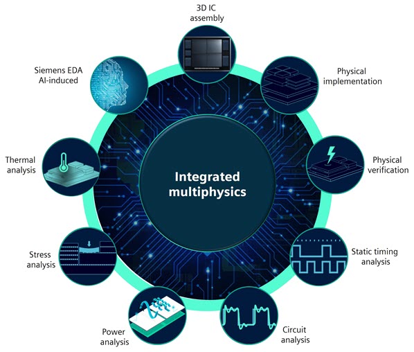
At Siemens EDA, our answer to these demands is the Calibre 3D IC solution. This suite of tools—Calibre 3DStack, Calibre 3DStack Advanced, Calibre 3DThermal, Calibre 3DStress and Calibre 3DPERC—address the increasingly complex physical verification hurdles inherent in modern 3D IC design. Our integrated multiphysics verification environment spans from the transistor up through the die, board, package and ultimately, the final system-level operating environment, ensuring every aspect of a 3D IC design is physically, electrically, thermally and mechanically sound. Figure 1 illustrates the various analysis domains that can be integrated within a multiphysics simulation framework, enabling a holistic understanding of system behavior.
Achieve comprehensive physical verification for 3D ICs with Calibre 3DStack
Siemens EDA established an early, market-leading position in the 3D IC space through the introduction of Calibre 3DStack. As 3D IC technology progresses, we’ve expanded our capabilities with Calibre 3DStack Advanced.
Calibre 3DStack Advanced includes all of the core 3DStack capabilities while introducing new features that tackle the most complex 3D IC verification tasks. It addresses emerging requirements, like die-to-die P2P current density checks, 3D antenna verification and automated DRC for interface layers. Key features include:
- All basic physical and connectivity checks, including 3D extraction
- Inter-chiplet antenna checking
- Inter-chiplet DRC checking
- Calibre 3DPERC checking
- Enhanced control over custom checks
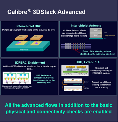
For example, the left image in figure 2 demonstrates how layers from within a die can be projected onto an interposer to verify both the alignment and DRC impact of interface layer interactions on an interposer. The right image illustrates the inter-chiplet antenna checking on a fully assembled 3D IC with multiple stacked chiplets.

The value of Calibre 3DStack Advanced is evident in its ability to perform complex verification operations that are required to ensure cutting-edge 3D IC designs meet stringent manufacturing and reliability specifications. Figure 3 highlights the key capabilities of Calibre 3DStack Advanced, including inter-chiplet DRC, inter-chiplet antenna checking, 3DPERC enablement for ESD effects and advanced DRC, LVS, and PEX for 2.5D/3D IC systems.
From point tools to integrated flows
Integrated 3D IC solutions can improve the efficiency and turnaround times in your design and verification workflows as compared to traditional, piecemeal solutions. The Calibre tools all share a foundation on proven Calibre interfaces, so users already familiar with the Calibre ecosystem need minimal training. Our tools are designed for interoperability, seamlessly integrating into existing workflows, a stark contrast to other products that may create workflow silos. The Innovator3D IC solution is an advanced graphical cockpit used to interactively design and debug your 3D IC assembly and launch Calibre 3D IC tools. Exploring floorplan variations and building complex models is straightforward through a combination of intelligent automation in the interface and support for the flexible 3DSTACK+ or 3Dblox languages. Innovator3D IC provides an interactive environment for constructing complete package designs and performing multiphysics analyses from a single, unified interface. This integrated approach enables designers to construct a true digital twin of a design that can be analyzed and optimized across a multitude of workflows and analysis types. This digital twin model can seamlessly navigate the entire design and analysis workflow, from initial concept to final product, providing an unprecedented level of insight and control. Figure 4 shows cross-sectional diagram of a complex 3D IC package, featuring an interposer, stacked HBM (high bandwidth memory), and multiple stacked ASIC (application-specific integrated circuit) chiplets. Innovator3D IC, along with the Calibre 3D IC verification tools, can model this structure under comprehensive multiphysics analyses from the early block-level concept all the way down the transistor-level structures present at tape-out.

Calibre 3DThermal, Calibre 3DStress, and Calibre 3DPERC are core components of this integrated multiphysics workflow and are integral to modeling your product accurately. The introduction of these tools for advanced package technology is critical, as the move to full 3D ICs with hundreds of chiplets introduces new concerns: thermal hotspots, mechanical stress and reliability issues.
Optimize 3D IC thermal performance with Calibre 3DThermal
One of the most pressing issues in 3D IC design is thermal management. The high power density and stacked nature of 3D ICs lead to significant thermal gradients and interactions between dies, which can severely impact performance and reliability. Figure 5 visually represents the critical thermal challenges in 3D IC design, showing how hotspots on individual dies (left) propagate and create significant thermal gradients across stacked dies (right), emphasizing the need for effective thermal management.

Safety margins that were applied in 2D designs do not easily transfer to advanced 3D packages because the runtime interactions between the dies are not easily predictable. You must accurately characterize these behaviors with simulation to correctly model the true thermal profile and impacts of a given package configuration and switching activity.
Watch Intel Foundry describe their 3D IC thermal workflow with Calibre 3DThermal.
Calibre 3DThermal offers a comprehensive set of features for thermal analysis throughout the entire design flow, from concept to signoff. Leveraging an optimized 3D solver from Simcenter Flotherm, Calibre 3DThermal delivers highly accurate and efficient thermal simulations. Calibre 3DThermal was introduced to make thermal analysis accessible to IC design and verification engineers. You don’t need to be a thermal or mechanical engineering expert with extensive CAD modeling experience to set up and run these tools on your package design. Tasks such as meshing and 3D model construction are largely automated, drastically reducing the learning curve and allowing a broader range of engineers to conduct these critical analyses (figure 6).

Advanced automation features, such as adaptive power map compression, highly accurate layout-based thermal property modeling and hotspot detection put powerful thermal capabilities in the hands of IC designers.
Another significant benefit of Calibre 3DThermal is its bi-directional model transfer capability with Simcenter Flotherm. This allows chip designers to easily pass detailed die-level models to system-level thermal engineers, who can then provide realistic boundary conditions back to the chip designer. This integrated workflow not only saves time but also improves accuracy, communication and overall optimization of the development process.
Conquer mechanical stress with Calibre 3DStress
Complex stacks, heterogeneous dies and intricate assembly flows all contribute to thermo-mechanical and material-driven stress that can lead to issues like die warpage, cracking, delamination and even variations in electrical characteristics.
Calibre 3DStress helps design teams uncover, understand and manage these stress-induced reliability risks in 3D ICs and chiplet-based architectures. Traditional 2D sign-off tools and even many package-level simulators, often can’t detect how these stresses manifest at both the device and assembly level. This can result in failure modes or degraded reliability being discovered late in development or, worse, after product manufacturing.
Learn more by reading our technical paper: Thermo-mechanical stress on active chiplets in a 3D IC heterogeneous package assembly.
Designers use Calibre 3DStress to address these gaps by combining automated extraction of material properties and layout data, detailed multi-scale modeling and a highly scalable solver (figure 7). The tool provides actionable results quickly, supporting both rapid prototyping and dependable final sign-off. Design teams can minimize manual intervention and reduce errors through automated context capture. The robust finite element analysis (FEA)-based modeling accounts for the complete physical context, including interfaces and detailed device-level effects, providing a true picture of stress distribution. Intuitive, actionable output, such as high-resolution stress maps and overlays in Calibre RVE, allows teams to engage directly with their results and pinpoint effective mitigation options.

Watch how STMicroelectronics used Calibre 3DStress for chip-package stress analysis.
Read more about Calibre 3DStress in our technical paper: Advanced stress analysis for reliable 3D IC design
Manage electrostatic discharge risks with Calibre 3DPERC
Electrostatic discharge (ESD) failures are a persistent and costly issue and conventional reliability verification methods are no longer sufficient for advanced multi-die architectures.
For 2.5D or 3D architectures, reliability verification grows exponentially in complexity. Many modern 3D ICs combine dies built on diverse technology nodes, designed by different teams and manufactured by separate foundries. Traditional methods, built for single-die designs, fail to capture these nuanced interactions. We offer an integrated workflow for 3D IC reliability verification. Innovator3D IC prepares 3D IC designs and generates netlists, which Calibre 3DStack uses to build full multi-die connectivity models. Calibre 3DPERC leverages these models for advanced reliability checks, including ESD path validation, point-to-point resistance and current density analysis. This seamless integration eliminates errors and ensures consistent verification throughout the process. Figure 8 illustrates running an ESD check across a stacked assembly.

Download our technical paper, System-level reliability verification for 2.5D/3D ICs using Innovator3D IC and Calibre 3DPERC to learn more about verifying ESD protection in heterogenous die integrations and inter-die connectivity.
Shift left 3D IC verification
All the Calibre 3D IC solutions fit smoothly into every phase of the design lifecycle. Early-stage engineering benefits from quick “what-if” analyses, while flexible scenario analysis supports optimal device placement and material selection as the design matures. At sign-off, comprehensive verification ensures the entire stack meets defined stress criteria, significantly reducing the risk of late surprises. Furthermore, Calibre 3DStress and Calibre 3DThermal tools support device-level back-annotation, allowing physical simulated effects to be directly fed into electrical extraction and circuit simulation, thereby closing the loop for robust 3D IC development.Figure 9 illustrates how Calibre 3D IC solutions enable device-level back-annotation to shift left, feeding simulated thermal effects from a 3D IC package (right) into electrical extraction and circuit simulation (left) to ensure robust 3D IC development.

Calibre 3DThermal and 3DStress represent a fundamental shift in multiphysics analysis, moving it “left” into the concept phase of design. With potentially hundreds or thousands of chiplets in a single package, finding the optimum floorplan, placement and electrical design without making risky assumptions is paramount. As designs progress from concept to sign-off, the boundary conditions and physical makeup of the design mature from uniform blocks to hyper-accurate, instance-level digital twins based on complete GDS or LEF/DEF databases. This enables accurate electro-thermo-mechanical co-simulation throughout the entire design cycle.
Strength through partnerships
The development of our Calibre 3D IC tools is a testament to close collaboration with customers and leading foundries. The partnerships ensure that our solutions are scalable, flexible and seamlessly integrate with any workflow, which is why Calibre 3DStack has consistently been the preferred tool for 3D IC physical verification.
The Calibre 3D IC solution provides a comprehensive, automated and integrated platform for physical verification, thermal analysis and stress analysis, enabling engineers to confidently design and verify complex 3D ICs and chiplet-based architectures, ensuring reliability and accelerating time to market.