2.5/3D IC designers! Don’t get hung up on latch-up!
By Dina Medhat
Latch-up is modeled as a short circuit (low-impedance path) that occurs in an integrated circuit (IC). It can destroy an IC due to over-current created by interactions between parasitic devices (PNP and NPN). As designers, your job is to stop latch-up before it can happen, by finding and resolving those conditions in your layouts. As you know, there are fundamental latch-up rules, which are the local latch-up design rules that focus on physical dimension rules associated with the parasitic pnpn network. Then there are the advanced latch-up design rules, which fall into two main categories: (1) external latch-up rules, and (2) mixed-voltage rules.
Applying these advanced latch-up design rules requires knowledge of both the external injection sources and voltage. The most common method used to provide this information to your electronic design automation (EDA) tools is to use manual layout markers. However, such markers present challenges even in 2D designs, because hey! we’re human, and designers sometimes misplace some markers, especially when working on full chips in advanced technology nodes where there are many marker types. And if you’re a 2.5/3D IC designer, you know that managing a layout markers methodology becomes even more problematic in 2.5D and 3D designs. So, what do you do?
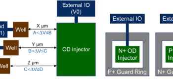
A key difference between 2D ICs and 2.5D/3D ICs is that the latter has two different IO types (external IOs and internal IOs). Such classification of IOs in 2.5D/3D ICs is essential for latch-up verification, because internal IOs have a pretty low latch-up risk. That means we can ignore them from a latch-up perspective, and focus only on verifying the external IOs. Really? Yes, really.
So, is there any methodology to differentiate between these two IO types automatically, and check only the external IOs for appropriate protection…without having to use those special layout markers? The short answer is yes.
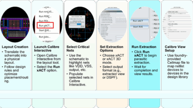
At Siemens EDA, we formulated a systematic methodology using the Calibre PERC reliability platform that consists of a topology-aware flow to address external latch-up design rules, and a voltage-aware flow to address mixed-voltage latch-up design rules. These flows can automatically identify external IOs from the assembly level, without using any special layout markers on the die level. Implementing an automated latch-up verification solution for 2.5/3D IC designs ensures correct and consistent protection, ensuring a more reliable product in less time.
Interested in the details? Download a copy of our technical paper, 2.5D/3D IC latch-up prevention: an automated verification strategy.