Okay, I released my design to the fab, now what? Design to Mask – Part 1
By Minghui Fan, Mentor Graphics
The design is finally sent to the fab, where it magically becomes real. Is it magic? Or is it practiced application of advanced computational lithography? Continue reading to learn about the advances in OPC and modeling that make it happen.

Here in the Calibre group we have worked closely with foundries for over a decade, so we’ve developed an intimate understanding of what it takes to prepare your designs for manufacturing. In this blog and in two more blogs to follow, we will offer some of the key lessons that we’ve learned about getting through the various post-tapeout stages with style. The Calibre tools reflect our close partnership with foundries in focusing on what is important to you as you go from early development to manufacturing.
Let’s assume you have just completed your design and are ready to hand off the design to the mask house. What steps do foundry engineers take to improve design yield? At the advanced and emerging process nodes, systematic defects as well as defects that arise from design-styles are becoming yield limiters. Current 193 nm immersion lithography simply cannot pattern 16 nm, 10 nm, or 7 nm features without distortion, even with multi-patterning. Lithographic systems are being pushed to their limits and foundries use ever more advanced materials and resists, yet they find themselves with marginal process windows that don’t support the semiconductor density scaling.
This process window problem is addressed by the foundry through the use of computational lithography software that alters the extremely complex and small layout geometries in order to make them manufacturable.
There are a few key components of computational lithography that make manufacturing of advanced-node layouts a success:
- Optical proximity correction (OPC) and resolution enhancement technology (RET) software that achieves the maximum possible process window
- Software, applications, and methodologies that allow foundries to increase their productivity thereby reducing development cycle times, complexity and costs
- Management of the Post Tape Out Flow so as to provide predictable and scalable turnaround times while minimizing computational costs
Let’s look at recent advances in the Calibre OPC and RET software and how this technology ensures the best possible yield.
Advances in OPC
While OPC has become essential in modern semiconductor manufacturing, designs on the latest processes need the most advanced OPC to overcome the patterning challenges we see at 28 nm and below. During OPC, edges in a layout are broken into fragments, each of which is iteratively adjusted by multiplying its edge placement error (EPE) with a carefully selected or calculated feedback. Traditional OPC assumes a one-to-one correspondence between each polygon fragment on a mask and its associated EPE on the wafer. That means that moving one fragment on the mask only impacts the associated EPE, and conversely, that the incremental displacement of a fragment on a mask can be estimated by its associated EPE during the OPC iterations.
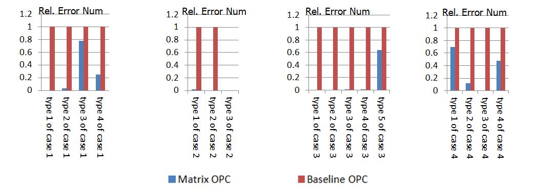
However, this approach breaks down at and below 28 nm because of the strong cross-coupling between neighboring fragments. So how do you get OPC to recognize the effect neighbor fragments have on each other? You use a full-chip matrix OPC. Matrix OPC incorporates the influence of neighboring fragments into the feedback control of fragment movements for full-chip OPC. Calibre invented it, and still offers the only computationally feasible solution. It calculates the movements of all polygon fragments on the mask collectively and adds zero overhead to the OPC turnaround time!
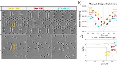
Another challenge in OPC has been finding the optimal placement of sub-resolution assist features (SRAFs) that gets you the process window you need while working within the manufacturability (consistency) and computational/development constraints. SRAF placement had moved from rules-based to model-based approaches a few years ago. However, there has been a growing realization in the industry that neither the rule-based nor the model-based approach is sufficient by itself. Calibre’s solution to the problem is in developing a hybrid approach that takes the best of both approaches. This approach is becoming the industry standard at 14 nm and below since it is the only approach that provides you with the needed process margin while meeting the consistency requirements. For more details on this approach, download this paper that was presented at SPIE Advanced Lithography “A Novel Full Chip Process Window OPC Based on Matrix Retargeting.” [URL to come]
Modeling Innovations
New process effects are a key challenge for manufacturing at 28 nm and below and have driven the need for accurate and fast simulation of 3-D phenomena associated with the mask, wafer, and resist. I will talk about two specific phenomena in this space and our solutions.
Patterns on the wafer implant can cause light reflection and scattering back to the photoresist layer, which leads to large edge placement errors. In the past, this was resolved by using a bottom anti-reflective coating (BARC) layer. However, the BARC adds cost and creates yield concerns.
So we developed an OPC solution for these layers in the form of under-layer topography models, which capture the complex array of wafer topography effects. These models are being expanded to better represent the impact of active FinFETs and the results for pre- and post-poly layer implant models have been excellent. The Calibre solution has found industry-wide deployment at 14 nm.
There is also a new focus on the photoresist model. The 14 and 10 nm nodes feature extensive use of negative-tone develop (NTD) resist processes for the patterning of metal and via layers. These NTD resist processes have different properties than the traditional positive-tone (PTD) processes. We developed new modeling capabilities to support NTD that result in a > 2X improved accuracy in predicting wafer results. We also improved the prediction of resist toploss and scumming as well as SRAF printing for both PTD and NTD cases.
These are only a few examples of the innovations in our OPC and RET sets of tools. We continue to invest and develop new and exciting technologies. Of course, all of these technologies drive a computational burden on both development and production. In my next blogs, I will talk about what we have been doing to manage that burden for you.