SRAM physical verification – Why does it have to be so hard? (Hint: it doesn’t)
By James Paris and Elven Huang – Mentor, A Siemens Business
Checking SRAM IP placements can be tricky, even for experienced designers. Adding pattern matching to your flow simplifies the process while improving the results. And it’s easy to update when you add new IP.

Static random-access memory (SRAM) structures are assembled in a physical design using a set of specific intellectual property (IP) blocks that abut or overlap one another in a specific arrangement that matches the circuit specifications. They’ve always been a little harder to verify because of differences (like smaller features sizes) between memory and traditional logic structures, but at advanced nodes, designers are facing a whole new level of difficulty.
But wait…don’t foundries supply SRAM libraries containing IP that they’ve certified for both functionality and a specific process node? What’s changed?
Because SRAM cells involve multiple layers, and contain many different geometry shapes with various dimensions, it’s always been the case that it’s nearly impossible to cover all potential placement issues with design rules. A lot of complex (and time-consuming) solutions have been developed over the years, including the use of marker layers and “nearly” duplicate design rules for regions of the design that contain the memory blocks. None of these solutions, however, have the ability to detect IP manipulation, placement overlaps, floating shapes, or unintended interactions. Prior to 20 nm, those mistakes were acceptable, because the manufacturing team could usually make adjustments during the manufacturing process to avoid any yield issues.
At 16 and below, that margin has evaporated. Mistakes in the assembly of the memory blocks or in the application of the appropriate rules to the right design data can result in catastrophic failures after manufacture.
What kind of issues are we talking about? Here’s a few of the more common ones:
- Misuse of SRAM types—Because there are many SRAM types for each node, designers can use a corner cell from type A in a SRAM block of type B, and not even realize it
- Misalignment—misalignments of placed cells can be as small as 1 nm, making the shift very difficult to detect
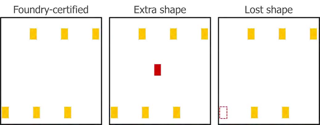
- Shape changes—design teams sometimes change the polygon shapes from the foundry-supplied SRAM cell, add/delete polygons from a compiled SRAM block, or shift polygons within a cell.
Thankfully, for every new challenge, there is a new solution. Unlike traditional DRC that is dedicated to one-dimensional checks such as width and space, the Calibre Pattern Matching verification methodology can evaluate a pattern consisting of multiple polygon shapes, and check multiple layers. That allows it to quickly and accurately identify IP manipulation and external interactions, and makes it easy to update when new IP elements are added.
Using an assembled SRAM block that includes all of the necessary elements, individual cells (such as bitcell (core), edge, top, bottom, corner, etc.) are converted to a pattern and stored in the pattern library. The stored patterns are tested against existing SRAM structures, and new patterns are added until every part of the entire memory structure matches a pattern.
Once the SRAM pattern library is established and verified, you can use it in your Calibre physical verification flow to automatically validate all SRAM IP placements, providing you with confidence that all SRAM structures are correctly implemented in your design.
Of course, that’s the simple explanation. If you’d like a few more details and some handy diagrams, download a copy of our white paper, SRAM Physical Verification with Calibre Pattern Matching.