CMP Modeling: Improving Manufacturing Results during Design
By Jeff Wilson and Ruben Ghulghazaryan – Mentor, A Siemens Business
Accurate CMP models and simulation are crucial to both design process optimization and manufacturing success. Calibre CMPAnalyzer tools support CMP model building, multi-layer full-chip CMP simulation, and hotspot detection and analysis.
Used to improve wafer planarity prior to integrated circuit (IC) assembly, chemical-mechanical polishing (CMP) has been a key component of IC manufacturing for more than two decades. However, with the scaling down of process technology nodes, planarity variations of just a few nanometers can have a significant impact on manufacturing success. Over- and under-polishing, dishing, and erosion can lead to defects in the final products.
To prevent these kinds of failures, companies traditionally created test wafers in which the CMP process could be refined before it was used in production. However, multi-patterning requirements have driven up the cost of advanced node lithography, making it impractical to use test wafers at the same rate as before.
Enter the use of CMP modeling. CMP modeling has become a cost-effective means of detecting and correcting CMP “hotspot” layout configurations during the design process, before actual manufacturing begins.  In addition, CMP modeling can help designers improve the design process for future designs, by identifying problematic layouts that should be avoided, or by recognizing when and how fill can be optimized to prevent manufacturing issues.
Of course, creating an accurate CMP model is crucial to this process. Geometrical properties of the patterns on the layout must be extracted, and then predictions generated for the post-polishing thickness variation of each pattern, depending on its position on the chip. A good CMP model must not only simulate polishing results for multiple materials due to the patterns’ geometry specifics, but also capture long-range polishing effects (like pad pressure and bending) specific to a given CMP process. These predictions are then calibrated against measurement data collected from test chips, to select model parameters that best reflect actual foundry process conditions.
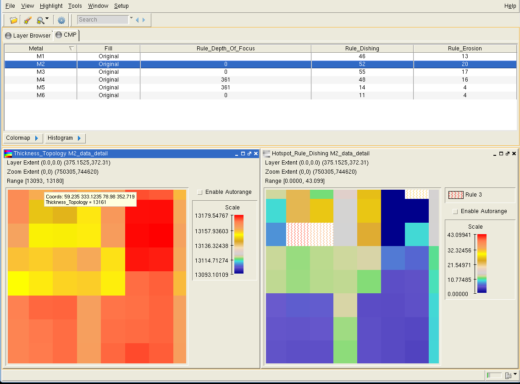
The Calibre® CMP ModelBuilder tool supports models for a variety of deposition processes, generating post-deposition profiles for polishing. Numerous CMP stop conditions used by CMP tools are supported by the simulator, allowing users to select the one appropriate for their process. Once the CMP model is built, the Calibre CMPAnalyzer tool provides automated multi-layer CMP simulation, hotspot detection, and analysis possibilities. It takes as input the GDS or OAS file of a design, layer numbers that must be simulated, and the best recipe file of the process created by the Calibre CMP ModelBuilder tool.
CMP modeling is a powerful tool that enables design teams to detect potential CMP hotspots prior to manufacturing by providing visualization and analysis of simulated CMP. CMP simulation also contributes to the continuous improvement of the design process by enabling designers to tune dummy fill solutions and enhance RC extraction accuracy, among others.
To learn more about the specifics of the CMP modeling process, and how the Calibre CMP ModelBuilder tool can help you develop your own CMP models, download our white paper, Building CMP Models for CMP Simulation and Hotspot Detection


