Say Goodbye to Messy Designs: Flat vs. Hierarchical Design Methodology
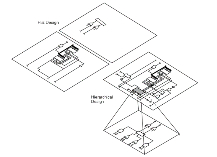
Most people are familiar with Flat Designs, it is usually a single schematic sheet that includes the entire circuit, and it can be divided into multiple sheets.
While this is usable for some designs, when dealing with larger projects and when work must be split across multiple designers, that is when the hierarchical design approach come to the rescue.
Below is an illustration of the Flat Design versus the Hierarchical Design Structure for better visualization.
Bigger designs mean more circuits, more effort, and more complexity, as a result, this can lead to more errors.
However, this doesn’t always need to be the case – we have got your back.
Hierarchical designs are used to organize your schematic and reuse your circuits without the need to re-create them which eliminate the probability of errors and yields a well-organized design.
Let’s understand the hierarchical design methodology.
What is Hierarchical design? Hierarchical design is a schematic representation to better organize your PCB designs. There is more than one approach to create a hierarchical design.
There are Top-Down and Bottom-Up Design Methodologies, sometimes a combination of both can also be used.
So, let’s dig deep and see the difference between these two design methods.
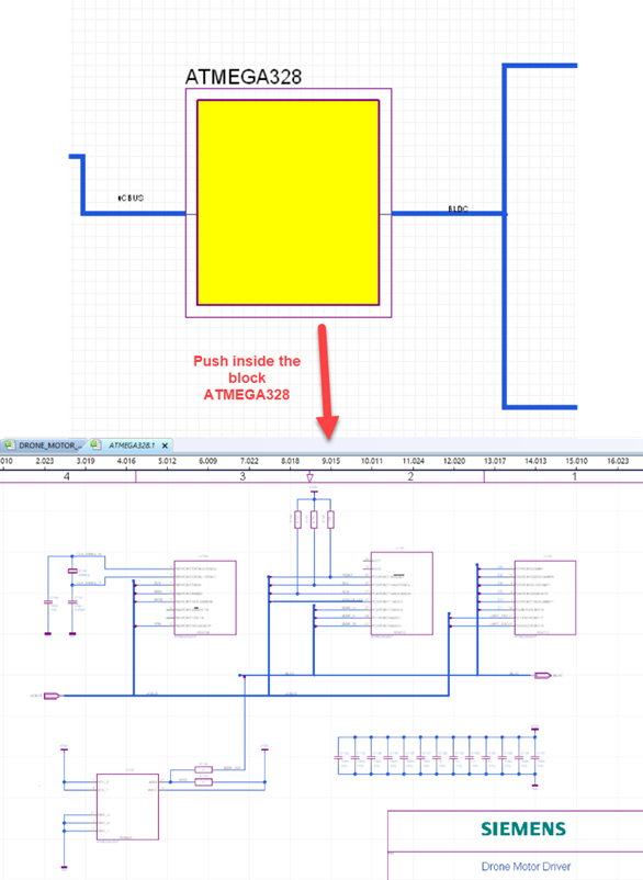
The Top-Down design focuses on creating the block symbol first and then pushing inside to add the circuitry and connections, while the Bottom-Up design creates the circuitry first and add all connections before generating the block symbol itself.
Below is an example of how a hierarchical block looks like in a schematic design.
In Xpedition™ Designer there are some rules that need to be considered when working with hierarchical designs.
The first rule is that all nets within a block are local, therefore same name nets in different blocks are not connected by default.
Also, all nets from within the hierarchy that need to connect to the outside must use ports on the schematic and use pins on the hierarchy symbol to create that connectivity, naturally those ports and pins should have matching names.
It is important to remember one exception to the hierarchical connectivity rule which indicates that signals that are connected to Global connectors (VCC, GND, etc..) are connected within the whole design without the need for pin/port connection.
If you’d like to learn more about Hierarchical Designs in the Xpedition Enterprise™, you can take our on-demand training course Schematic Entry in the Xpedition Flow. This course is also offered in instructor led format by our industry expert instructors and can be tailored to address your specific design goals. Also, you can now earn a digital badge/level 1 certificate by taking our Schematic Entry in the Xpedition Flow Exam. If you successfully pass the Level 1 Certification Exams, you can display your digital badge on LinkedIn or your email signature.
For additional questions or assistance on this topic, contact a Siemens representative at xceleratoracademy_eda.disw@siemens.com.
Author: Angela Emil , Customer Training Engineer, Siemens EDA Learning Services


Comments
Leave a Reply
You must be logged in to post a comment.
Hierarchical design is a schematic representation for organizing PCB designs, using Top-Down and Bottom-Up methodologies, or a combination of both, to improve organization and efficiency.