Leveraging fault simulation for manufacturing test

Manufacturing test for ASICs remains a critical part of the development lifecycle, ensuring the delivery of defect free silicon. This is true for both safety critical ICs targeting automotive, industrial, mil-aero and markets where high-reliability is a must.
Background
The goal of manufacturing test activities is to ensure no defects exist during the fabrication of the silicon die. Testing is performed after fabrication using a suite of test vectors and dedicated scan hardware to identify defects in the silicon. Prior to fabrication, test engineers define the test vectors and hardware required to test each part of the design. Inserted test hardware adds no value to the functional objectives of the design. Therefore it is critical that manufacturing test capabilities have minimal impact to power and area while achieving the defect coverage target.
Manufacturing test has been around for decades, but recently, the challenge of achieving sufficient defect coverage in safety-critical and high-reliability designs is exacerbated. This challenge is due to the exponential rise in complexity of semiconductors being created for safety-critical markets in part by the evolution of autonomous driving, industrial robotics, and more. To address this challenge, companies are moving to advanced defect modeling such as cell-aware technology and other physically driven models. These advanced fault models are being applied on top of transition delay, path delay, bridging, and the traditional stuck-at fault model.
Leveraging functional patterns to improve defect coverage
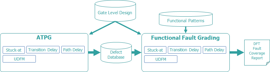
Historically, ATPG generated vectors struggle with latch constructs or multi-cycle paths. Additionally, speed paths where scan isn’t an option and untested logic in scan implemented blocks are also troublesome. Safety-critical and high reliability designs required coverage on these undetectable defects. Fortunately, functional patterns are leveraged to “top-off” ATPG coverage and achieve a very low defects parts per million (DPPM). But how is the effectiveness of a functional pattern evaluated? Traditionally, gaps in ATPG covered are reviewed via expert judgement. In some instances, traditional circuit simulation is leveraged to sanity test a small subset of uncovered defects. Figure-1 shows the workflow where fault simulation, commonly known as fault grading, is performed to complement ATPG.
Deploying fault simulators
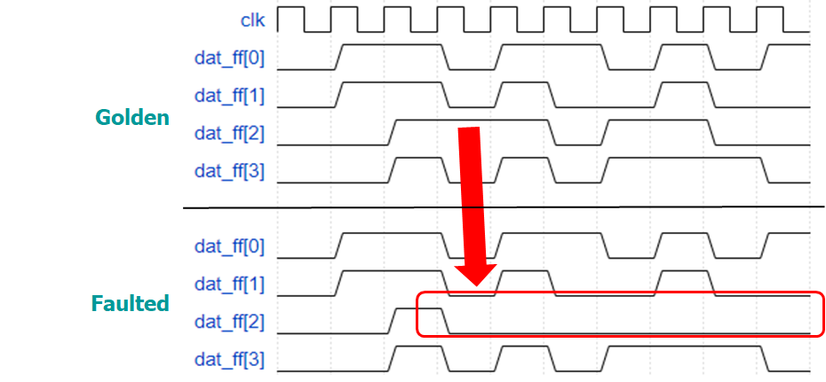
Fortunately, fault simulators have been created to help fill the void by offering concurrency across multiple fault model variants (Stuck-at, transition delay, user defined). Additionally intelligent defect injection and propagation are built-in which automates when and what fault type to inject. Leveraging functional patterns, defects are injected and propagation is evaluated to identify if an observe point is reached, indicating that particular defect will be detectable with the supplied functional pattern. Figure-2 shows a timing diagram and the impact of a stuck-at 0 fault on a golden functional pattern.
Customers who are developing safety-critical or high-reliability applications will likely have extremely low DPPM targets. Test engineers must be creative in closing that last bit of defect coverage. The entrance of fault simulators have help immensely in evaluating the coverage achieved for functional patterns and has proven to be an ideal solution for topping-up ATPG defect coverage. Please reach out if you are interested in learning more about Siemens industry leading test solutions.