Part 7: The 2014 Wilson Research Group Functional Verification Study
ASIC/IC Design Trends
This blog is a continuation of a series of blogs related to the 2014 Wilson Research Group Functional Verification Study (click here). In my previous set of blogs, I focused on FPGA design and verification trends. I now will shift the focus of this series of blogs from FPGA trends to ASIC/IC trends.
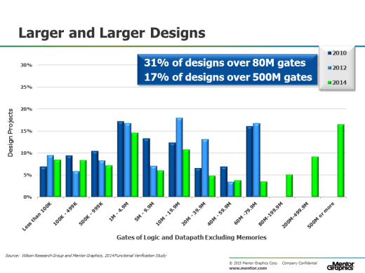
In this blog, I present trends related to various aspects of design to illustrate growing design complexity. Figure 1 shows the trends from the 2007, 2012, and 2014 studies in terms of active ASIC/IC design project by design sizes (gates of logic and datapath, excluding memories). The 2014 study added more resolution in identifying larger design sizes (up to 500M or more gates), while the 2012 studies’ upper bound was limited to 60M or more gates.
 Figure 1. ASIC/IC Design Sizes
The key takeaway here is that the electronic industry continues to move to larger designs. In fact, 31 percent of today’s design projects are working on designs over 80M gates, while 17 percent of today’s design projects are working on designs over 500M gates.
But increased design size is only one dimension of the growing complexity challenge. What has changed significantly in design since the original Collett studies is the dramatic movement to SoC class of designs. In 2004, Collett found that 52 percent of designs included one or more embedded processors. Our 2014 study found that the number of designs with embedded processors had increased to 71 percent. Furthermore, 45 percent of all designs today contain two or more embedded processors, while 12 percent of today’s designs include eight or more embedded processors. SoC class designs add a new layer of verification complexity to the verification process that did not exist with traditional non-SoC class designs due to hardware and software interactions, new coherency architectures, and the emergence of complex networkon-a-chip interconnect.
In addition to the increasing number of embedded processors contained within an SoC, it is not uncommon to find in the order of 120 integrated IP blocks within today’s more advanced SoCs. Many of these IP blocks have their own clocking requirements, which often present new verification challenges due to metastability issues involving signals that cross between multiple asynchronous clock domains.
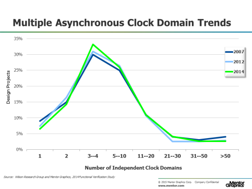
In Figure 2, we see that 93 percent of all ASIC/IC design projects today are working on designs that have two or more asynchronous clock domains.
 Figure 2. Number of Asynchronous Clock Domains in ASIC/IC Designs
One of the challenges with verifying clock domain crossing issues is that there is a class of metastability bugs that cannot be demonstrated in simulation on an RTL model. To simulate these issues requires a gate-level model with timing, which is often not available until later stages in the design flow. However, emerging static clock-domain crossing (CDC) verification tools can identify clock domain issues directly on an RTL model at earlier stages in the design flow.
In my next blog (click here) I plan to discuss the growing ASIC/IC design project resource trends due to rising design complexity.
Quick links to the 2014 Wilson Research Group Study results
- Prologue: The 2014 Wilson Research Group Functional Verification Study
- Understanding and Minimizing Study Bias
- Part 1 – FPGA Design Trends
- Part 2 – FPGA Verification Effort Trends
- Part 3 – FPGA Verification Effort Trends (Continued)
- Part 4 – FPGA Verification Effectiveness Trends
- Part 5 – FPGA Verification Technology Adoption Trends
- Part 6 – FPGA Verification Language and Library Adoption Trends
- Part 7 – ASIC/IC Design Trends
- Part 8 – ASIC/IC Resource Trends
- Part 9 – ASIC/IC Verification Technology Adoption Trends
- Part 10 – ASIC/IC Language and Library Adoption Trends
- Part 11 – ASIC/IC Power Management Trends
- Part 12 – ASIC/IC Verification Results Trends
- Conclusion: The 2014 Wilson Research Group Functional Verification Study


Comments