Part 2: The 2014 Wilson Research Group Functional Verification Study
FPGA Verification Effort Trends
This blog is a continuation of a series of blogs related to the 2014 Wilson Research Group Functional Verification Study (click here). In my previous blog (click here), I focused on FPGA design trends. In this blog, I present findings from our study related to the effort spent in verification.
Directly asking study participants how much effort they spend in verification will not work. The reason is that it’s hard to find a paper or article on verification that doesn’t start with the phrase: “Seventy percent of a project’s effort is spent in verification…” In other words, the industry is already biased to respond with this effort value. Yet, there are really no creditable references to quantify this value.
I don’t believe that there is a simple answer to the question, “How much effort was spent on verification in your last project?” In fact, I believe that it is necessary to look at multiple data points derived from multiple questions to truly get a sense of effort spent in verification. And that’s what we did in our functional verification study.
Total FPGA Project Time Spent in Verification
To try to assess the effort spent in verification, let’s begin by looking at one data point, which is the total project time spent in verification. Figure 1 shows the trends in total percentage of FPGA project time spent in verification by comparing the 2012 Wilson Research Group study (in dark blue), and the 2014 Wilson Research Group study (in light blue).
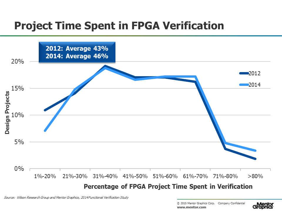
Figure 1. Percentage of FPGA project time spent in verification
Between the years 2012 and 2014 the industry did see a seven percent increase in the average time an FPGA project spends in verification. Historically, FPGA projects have spent less time in verification than ASIC/IC projects. The FPGA project strategy has traditionally been to get to the lab as soon as possible, and then iterate on issues in the lab. In a future blog I’ll show data that indicates this strategy does not necessarily yield good results in terms of meeting project schedule or quality objectives. Also, this lab-focused approach to FPGA verification becomes less effective as FPGA complexity increases.
Peak Number of Design and Verification Engineers
Perhaps one of the biggest challenges in design and verification today is identifying solutions to increase productivity and control engineering headcount. To illustrate the need for productivity improvement, we discuss the trend in terms of increasing engineering headcount for FPGA projects. Figure 2 shows the mean peak number of design and verification engineers working on an FPGA project. Again, this is an industry average since some projects have many engineers while other projects have few.
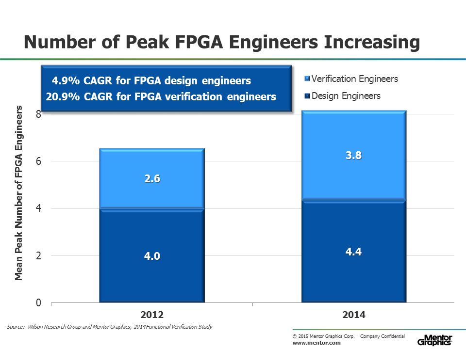
Figure 2. Mean peak number of engineers working on an FPGA project
You can see that the compounded annual growth rate (CAGR) for the peak number of FPGA design engineers between 2012 and 2014 was 4.9 percent, while the CAGR for the peak number of FPGA verification engineers was 20.9 percent. This huge demand for verification engineers on FPGA projects is one indicator of growing verification complexity in FPGA designs. Also, note that the ratio of design engineers versus verification engineers is approaching 1-to-1. This similar trend happened on traditional ASIC/IC designs in 2012.
In my next blog (click here) I focus on the time that FPGA design and verification engineers spends in various task.
Quick links to the 2014 Wilson Research Group Study results
- Prologue: The 2014 Wilson Research Group Functional Verification Study
- Understanding and Minimizing Study Bias
- Part 1 – FPGA Design Trends
- Part 2 – FPGA Verification Effort Trends
- Part 3 – FPGA Verification Effort Trends (Continued)
- Part 4 – FPGA Verification Effectiveness Trends
- Part 5 – FPGA Verification Technology Adoption Trends
- Part 6 – FPGA Verification Language and Library Adoption Trends
- Part 7 – ASIC/IC Design Trends
- Part 8 – ASIC/IC Resource Trends
- Part 9 – ASIC/IC Verification Technology Adoption Trends
- Part 10 – ASIC/IC Language and Library Adoption Trends
- Part 11 – ASIC/IC Power Management Trends
- Part 12 – ASIC/IC Verification Results Trends
- Conclusion: The 2014 Wilson Research Group Functional Verification Study


Comments
Leave a Reply
You must be logged in to post a comment.
“lab-focused approach to FPGA verification becomes less effective as FPGA complexity increases”
Now _that_ is a big statement. Is there any data to back that up?
Hi Michael, Yes measured by rising debugging time trends in the lab. A lot more data to be released soon…