Plan to plan on planning effectively

In order to stay competitive in the digitalization age of manufacturing, design organizations of complex products must author, analyze, and manage manufacturing process plans more efficiently. They will also need to communicate the plans throughout their organization and extended enterprise more effectively.
Efficient planning requires understanding “What is it?”, “Can I build it?”, “How to best build it?” and “Where to best build it?” within a manufacturing organization. Unfortunately, within many organizations with their multi-departmental silos and deep-rooted domain isolation, answering these questions required bouncing between people and systems. Very inefficient. Ideally, a single solution that is integrated with design eco-systems such as Teamcenter, which is also comprehensive in its ability to support PCB Assembly Manufacturing would solve these efficiency problems.
What Is It?
Products are defined by mostly 3 key articles of information; eCAD, Bill of Materials (BOM), manufacturing notes from Design. eCAD describes the actual product model (e.g. Layer stackup, copper tracks locations, component locations, copper pads, holes locations, etc.). The Bill of Materials (BOM) describes approved components, specifically, for each eCAD component location (sometimes referred to as Reference Designator), should be placed on the PCB. Many times the BOM also includes the quantity of a specific component and descriptions of the component (e.g. 0805 100ohm 1% 5W resistor). Finally manufacturing notes from Design are additional documents that provide requirements or guidance to the manufacturing organization. It may include IPC Class requirements, materials to be used, testing requirements, etc.
Can I build it?
One must assess both process feasibility and production feasibility to answer the question of whether a product can be built within an organization. Process feasibility assesses specific process risk characterization on the design itself. Some process risks may include; stencil design risks, ensuring adequate thermal relief on through holes, via locations too close to solderable pads, etc. Production feasibility assesses the risk to the actual production of the assembly. Typically these risks include adequate spacing of components to ensure no collision risk during placement, access to test points and testability, component thermal profiling risk, heavy component dropoff on secondary side assembly, etc.
How to best build it?
How a product should be built is normally a function of Manufacturing Planning and Process Engineering determining the process and process steps for manufacturing. Typically this is represented in the process of taking the original design BOM (eBOM) and creating a “manufacturing” BOM (mBOM). An mBOM defines the additional parts, tools, processes needed to ensure the PCB and related BOM lines of components and parts are assembled in the best way. When there is a system that has built-in intelligence and a learning library, this process becomes more consistent and reliable, thus more effective.
Where to best build it?
Manufacturing planning, process engineering and/or production planners determined which production lines, stations, cells or process steps should be used. This is typically represented in a Bill of Process (BOP). For complex products, a product BOP and plant BOP may be defined. A product BOP contains components and sub-assemblies, as well as the recipe of operations and resources needed to build the product. A plant BOP consists of stations and cells with the list of operations that can be performed at a particular station. Finally, the related programs, recipes, profiles for the stations, equipment, cells should be generated. Documentation to ensure the right stations are performing according to the approved BOP should be created and available on the shop floor. A solution that has template BOPs for characterized products, customers, or design centers, then again a repeatable and reliable production can be achieved.
Planning in Electronics Manufacturing.
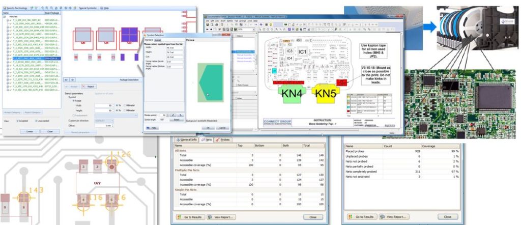
Siemens’ Valor Process Preparation solution provides this integrated solution, driving efficiencies into the design to manufacturing process, through to production preparation and execution.
In the next series of Blogs, we will deep-dive into each of the questions described above, so PCB Assembly manufacturers can truly achieve efficient manufacturing planning for cost-effective and reliable production.