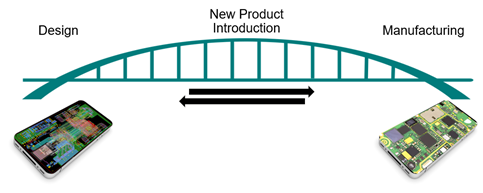
What is New Product Introduction (NPI) and How Does it Apply to PCBs?
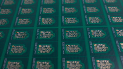
New product introduction, or NPI for short, is a structured process for transforming a product idea into a complete end-product that can be fully reproduced. In the electronic manufacturing process, refining a printed circuit board (PCB) design to the point it is production-ready is enormously demanding. It can be time-consuming and expensive, involving multiple iterations and requiring intense collaboration between the PCB designer and manufacturer. A robust NPI strategy reduces much of the complexity in designing a production for manufacturing and can save significant costs and time.
In general, regardless of the industry, NPI typically follows a six-stage process:
- Ideation – Identify the challenge or need and explore ideas for the solution.
- Definition – Define the product concept and requirements, evaluate potential market size and revenues, analyze feasibility
- Design – Create a detailed design and a bill of materials
- Testing – Build prototypes, test overall functionality and evaluate strengths and weaknesses
- Pre-production – Confirm that the product as designed can be manufactured on the production line at the required quality.
- Volume manufacturing – Produce sellable products and refine manufacturing to improve yield
While the phases are followed in order, there’s also a lot of back and forth – each stage of the process impacts, and is impacted by, the next one. For example, discoveries in testing and pre-production can prompt a return to the design stage. As the product progresses through each stage of NPI, the costs of changes and fixes rise. Most importantly, issues uncovered in pre-production (or worse, in manufacturing) are the costliest, as late-stage fixes waste significant time and materials.
The growing importance of NPI for PCBs
The pace of PCB new product introductions has increased exponentially over the past few years – and with it the need for a proper NPI process. It’s not just that PCBs are used in more and more products across numerous industries; it’s also that more PCBs are needed in those products. For example, consider how many PCBs are used in even the lowest-end cars today versus how many were used years ago. As new-model cars become increasingly connected to online services, the need for PCBs will continue to grow.
In parallel, increasing competition around electronic products like smartphones, TVs, home appliances, electric scooters, and bikes means manufacturers need to get to market quicker, with more product versions. The upshot: more PCB new product introductions in less time.
While contending with increased product variety and reduced lead times, PCB manufacturers also need to keep costs as low as possible to preserve their profit margins. With 80% of the costs of manufacturing is determined in the design and development phase, proper NPI can make a huge difference to a product’s commercial viability.
How are NPI principles applied to PCBs?
NPI spans PCB design and manufacturing, providing value for new boards as well as improved versions of existing ones. It involves:
- Understanding the manufacturing impact of a PCB design
- Optimizing the PCB design for volume production
- Communicating complete PCB design data to manufacturing
- Generation of manufacturing tooling, programs and documentation.
A rule of thumb is that the cost of fixing PCB design issues increases ten-fold with each step from development to testing to full-scale production. By integrating NPI as a core element in the PCB development and manufacturing process, manufacturers can mitigate many of the risks of production, such as quality problems, delays, and cost-overruns.
Explore Valor NPI with our Online Trial
Explore Valor NPI with our free online trial and find out how easy it is to implement the world’s most advanced DFM software. With no download or installation necessary, this simple guided tour provides immediate hands-on experience. Select your desired workflow:
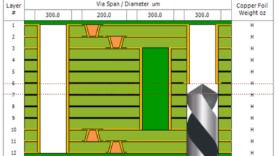
Key stages in the PCB NPI process
The PCB NPI process follows the same fundamental logic as NPIs in any industry (as described at the top of this article). But, due to the innate complexity of PCBs and the high costs of failure, the process is more complex and sophisticated.
PCB NPIs typically proceed through these stages:
- Define features, budget, functions, requirements
- Feasibility – Analyze preliminary design approaches, manufacturing success potential, timelines
- Development – Verify designs for manufacturability (DFM review), including and/all of the following reviews: design for assembly (DFA), design for testability (DTT), design for fabrication (DFF), design for reliability, design for x – excellence (DFX)
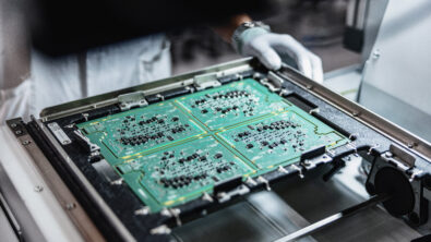
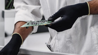
- Testing and pre-production – Production engineering, test overall design, functionality, manufacturability, quality
- Documentation – Produce the manuals, catalogs, sales and training materials, etc.
- Evaluation – Review product performance, get feedback from the customer
- Full-scale production – Volume manufacturing, reviews to improve yield and reduce costs
NPI benefits for PCBs
Electronic product designers and manufacturers that have adopted NPI are seeing significant pay-offs across almost every aspect of PCB development and production, including:
- Reduced re-spins — By ensuring that the PCB design fully meets all functionality and performance goals before it is transferred to assembly, NPI reduces or even eliminates re-spins. With an average cost of $28,000 per re-spin, this be a huge cost saver.
- Other production efficiencies – Following best practices for design for manufacturing and assembly (DFM / DFA) helps streamline the manufacturing process, improving production efficiency and reducing waste.
- Lower manufacturing costs – When the design team have easy access to manufacturer-specific manufacturability and assembly capabilities and constraints, they can make changes early on. This minimizes late-stage design changes and revisions and reduces the need for validation testing, saving manufacturing costs.
- Improved product quality – Implementing account design, engineering, and testing best practices, helps assure consistent, high product quality.
- Shorter time to market – Handling design errors, material compatibility problems, manufacturing defects, and other issues during NPI can speed design and pre-production, eliminate costly re-spins, and save days or even weeks of back and forth between design and manufacturing.
The Siemens approach to NPI
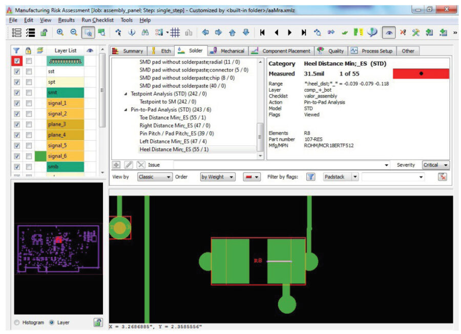
Design for manufacturing (DFM)is a crucial element in NPI. Implemented primarily in the design and testing stages, it ensures designs can be manufactured as designed, at the anticipated costs, and with the required quality and reliability.
Siemens’ Valor NPI software incorporates powerful DFM technology that enables manufacturing issues to be identified and corrected at the earliest stages of the NPI process. In addition to verifying that the design output data is suitable for the actual manufacturing capabilities and constraints of the specific manufacturer, the software prepares the design output data for streamlined hand-off to manufacturing process preparation.
Want to learn more about NPI?
Download a trial of Valor NPI today for an Xpedition workflow, or for use with Other EDA tools.