Practical machine learning for chip designers
Designers that spend their days creating new electronic chips push descriptions of their design through an elaborate flow of over 20 tools in order to get a verified product fabricated. Along the way, high-level concepts are captured in English-like programming descriptions that are transformed to lower and lower level abstractions until finally, they brush against the very limits of physics at almost the molecular level. For example, a graphics processor chip in a gaming computer can contain over 50 million transistors, yet its size is only 12 by 12 millimeters. Three grains of table salt stacked together are about 1 millimeter across.
At each step in the flow, designers apply verification techniques to ensure that the design works as expected. And, just to make sure, they throw random stimulus at the design just to guarantee that the design does not break when unexpected inputs happen. And if that is not enough, they run through millions of tests of the design under various environmental conditions, like temperature, to make sure that the chip will not fail in the field. If any of these tests fail, the flow starts over.
As the design winds its way through the tool flow, an amazing amount of data is collected. Even after fabrication, data about the quality of the design is fed back into the flow in order to improve manufacturing efficiency. The chip design flows can take many months to complete and design teams are always looking for ways to slice time off the development process in order to get to market before their competitors.
 Let’s look at what a chip design team does at the beginning of the process. Say that the team wants to create a chip that will part of a system that can recognize objects for an autonomous drive car. This is a typical example where applying machine learning (ML) within the chip is a potential solution.
Whenever the team ponders the application of ML to a particular problem, they typically start with the question, “Where can we get a massive amount of data?” This is because ML techniques use big data sets to train a neural network to find patterns in order to identify a particular object or situation or to uncover a data point that otherwise is not obvious to humans. In order to train the neural network, as much data as possible is desired. In this case, they need a massive database of photos that represent the typical objects that the system must identify out on the road. And they need labeled photos of objects in many orientations, in different lighting, weather conditions, confusing backgrounds, etc. In order to recognize a pedestrian, for example, they need millions of pictures of men, women, and children facing in all directions, in different lighting conditions (like sunshine or shade), and obscured through noise like rain or snow.
What if there is a one-leg pedestrian walking in a blizzard with her head is such a position that it looks like she is headless? Does the system recognize her as a pedestrian? This is an example of a “corner case” meaning it is possible but rare. For safety reasons, even corner cases are important.
After the system is trained within a lab, that knowledge is transferred into the chip so that it can be deployed in the autonomous driving system. Grossly simplified, the knowledge is a set of weights representing the probability that what the system sees matches an object that it has learned to recognize. This is also implemented in a neural net architecture on the chip.
Vendors that create the tools in the chip design and verification flow are also applying machine learning in order to improve results and to speed up the design and verification process. Instead of creating a chip, they create software algorithms to implement ML. Luckily, they have access to the data that a chip flow generates from real-world designs because customers and fabrication vendors volunteer that data in order to help tool vendors improve their solutions. For example, the vendors can run ML algorithms over terabytes of design data in order to pick out patterns or to reduce a massive set of possibilities to a few in order to speed up analysis. Instead of analyzing 1000 scenarios, tools can narrow that list down to 100 possibilities.
Applying AI to Chip Design Tools
Mentor, a Siemens business, has been employing ML to design tools for several years and continually explores the application of those techniques to improve the designer’s experience. Let’s explore a few of the ML-enhanced tools available today:
-
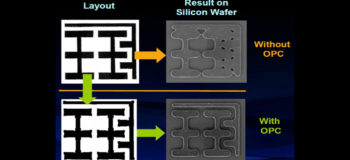
- Calibre® Machine Learning OPC. The dimensions of the features for the chip are so small, that the light wavelength is too large to “print” the features on silicon. Optical proximity correction (OPC) is a technique to account for this issue and to reduce fabrication errors.

-
- OPC requires many iterations to converge on a solution. By employing ML techniques the tool can eliminate many of those iterations and get to a result in much less time, using 2/3 of the computer resources. The ML algorithms are trained on data from the foundries that fabricate the chips and from real-world designs. Learn more here.
-
- Solido ML Characterization (MLChar) Suite. Chips employ models of blocks in the design that represent functionality like logic or memory in order to simulate the design before fabrication. These models need to be characterized to make sure that all the library elements perform correctly under all operating conditions (such as temperature and voltage). But the time it takes to completely characterize libraries can take months. MLChar uses ML methods to accelerate library characterization over 4 times faster. The tool works by creating a machine learning model from existing characterized seed data of a library. That model is then used to generate new characterization results for all operating conditions and also to validate all characterized data points in that library. Learn more here.
-
- Tessent® YieldInsight™. By analyzing failure reports from chip testing machines, ML techniques in this tool can detect the underlying root cause of failures in days instead of months. This is critical to improving the chip fabrication yield (number of chips on a wafer with no defects). Learn more here.
Additional tools within Mentor employ ML. In fact, there are other tools within the Calibre, Solido, and Tessent portfolios that use it. Just as ML has empowered amazing chips and electronic products, Mentor continues to explore the possibilities of leveraging these techniques and algorithms to provide innovative tools to the chip design community.
About the author:
Thomas Dewey is the content manager for custom integrated circuit design products at Mentor, a Siemens Business. Thomas has 30 years of electronic design automation (EDA) experience at Mentor ranging from engineering to technical marketing roles. He holds a BSEE degree from Oregon Institute of Technology.


